 ALLPCB


In the world of printed circuit board (PCB) manufacturing, achieving precision in solder paste deposition is critical for reliable assembly, especially when dealing with complex designs. If you're facing challenges with PCB design complexity due to varying component heights, step stencils offer a powerful solution. These multi-level stencils allow for customized solder paste volumes, ensuring optimal deposition for components of different sizes and heights on the same board.
In this blog, we’ll dive deep into how step stencils address component height variation and improve manufacturing outcomes for intricate PCB designs. Whether you're an engineer tackling advanced layouts or a manufacturer seeking better process control, this guide will walk you through the benefits, applications, and best practices of using step stencils for solder paste deposition.
What Are Step Stencils and Why Do They Matter in PCB Design?
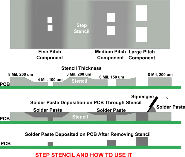
Step stencils, also known as multi-level stencils, are specialized tools used in surface mount technology (SMT) assembly to apply solder paste onto PCBs. Unlike traditional flat stencils, step stencils feature varying thicknesses across their surface. These thickness variations—created through etching or laser cutting—allow for precise control over the amount of solder paste deposited in different areas of the board.
Why does this matter? In modern PCB designs, components often vary significantly in height and size. For example, a board might include tiny 0201 resistors alongside larger connectors or ball grid arrays (BGAs). Applying a uniform layer of solder paste across such a board can lead to issues like insufficient paste for larger components or excess paste causing bridging on smaller ones. Step stencils solve this by tailoring paste volume to each component's needs, reducing defects and improving assembly reliability.
The Challenge of Component Height Variation in PCB Design Complexity
As electronics become more compact and feature-rich, PCB design complexity has skyrocketed. A single board may house components ranging from 0.4mm in height for chip resistors to over 2mm for power modules or connectors. This component height variation poses a significant challenge during solder paste deposition.
Using a standard stencil with uniform thickness often results in uneven paste application. For instance, small components might receive too much paste, leading to solder bridging, while larger components might get too little, causing weak joints. According to industry studies, improper solder paste volume can contribute to up to 60% of SMT assembly defects. These issues not only affect product reliability but also increase rework costs and production delays.
Step stencils tackle this problem head-on by allowing manufacturers to customize paste deposition. Thicker areas of the stencil deposit more paste for larger components, while thinner areas reduce paste volume for smaller ones. This targeted approach minimizes defects and ensures consistent soldering across the board.
How Multi-Level Stencils Work for Solder Paste Deposition
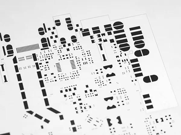
Multi-level stencils are engineered with precision to match the specific requirements of a PCB layout. The stencil is divided into "steps" or regions of different thicknesses, typically ranging from 0.1mm to 0.2mm for thinner areas and up to 0.25mm or more for thicker sections. These steps are created using advanced manufacturing techniques like chemical etching or laser cutting, ensuring accuracy down to a few micrometers.
During the SMT process, the stencil is placed over the PCB, and solder paste is spread across it using a squeegee. The varying thicknesses control how much paste passes through the apertures (openings) in each region. For example:
- A thinner step (e.g., 0.1mm) might be used for fine-pitch components like 0402 capacitors, depositing a minimal paste volume to prevent bridging.
- A thicker step (e.g., 0.2mm) could be applied for a BGA, ensuring enough paste for proper joint formation across its many pins.
This customization directly addresses the challenges of component height variation, making step stencils ideal for complex designs with diverse component types.
Benefits of Using Step Stencils in Complex PCB Designs
Step stencils offer several advantages for manufacturers and engineers dealing with intricate PCB layouts. Here are some key benefits:
1. Improved Solder Joint Reliability
By delivering the right amount of solder paste to each component, step stencils reduce the risk of weak or defective joints. For instance, a study in SMT assembly found that using multi-level stencils can decrease solder joint failures by up to 30% compared to standard stencils.
2. Reduced Defects and Rework
Issues like solder bridging, tombstoning, and insufficient paste are common in boards with component height variation. Step stencils minimize these defects by optimizing paste volume, saving time and resources on rework. This is especially valuable in high-volume production where even a 1% defect rate can lead to significant losses.
3. Compatibility with Mixed Technology Boards
Modern PCBs often combine surface mount and through-hole components, each requiring different paste volumes. Step stencils can accommodate these mixed technologies on a single board, streamlining the assembly process without the need for multiple stencils or manual adjustments.
4. Cost-Effective for Complex Designs
While step stencils may have a higher upfront cost due to their intricate manufacturing, they save money in the long run by reducing defects and improving yield. For complex PCB designs, the investment in a multi-level stencil often pays off quickly through enhanced production efficiency.
Applications of Step Stencils in PCB Manufacturing
Step stencils are particularly valuable in industries and applications where PCB design complexity is high. Here are some common scenarios where they shine:
- Consumer Electronics: Devices like smartphones and wearables pack a wide range of components into tight spaces. Step stencils ensure precise solder paste deposition for everything from microchips to power connectors.
- Automotive Electronics: With the rise of electric vehicles and advanced driver-assistance systems (ADAS), automotive PCBs often feature diverse components for power management and sensors. Multi-level stencils help maintain reliability under harsh conditions.
- Medical Devices: In medical electronics, where reliability is non-negotiable, step stencils support the assembly of compact, high-density boards with varied component heights.
- Industrial Equipment: Industrial control systems often use larger components alongside fine-pitch ICs. Step stencils provide the flexibility needed for consistent soldering across these boards.
Best Practices for Designing and Using Step Stencils
To maximize the benefits of step stencils in addressing PCB design complexity, follow these best practices during design and manufacturing:
1. Collaborate Early in the Design Phase
Work closely with your stencil manufacturer during the PCB design process. Share detailed information about component heights, pad sizes, and paste requirements. This ensures the stencil’s step levels are accurately tailored to your board’s needs.
2. Optimize Aperture Design
The size and shape of stencil apertures (openings) play a critical role in solder paste deposition. For fine-pitch components, use smaller apertures with a reduced area ratio (typically 0.5 to 0.6) to prevent excess paste. For larger components, increase the aperture size to ensure sufficient paste volume.
3. Test and Validate
Before full-scale production, run test batches using the step stencil to verify paste deposition across all component types. Use inspection tools like automated optical inspection (AOI) to check for uniformity and adjust stencil parameters if needed.
4. Maintain Stencil Quality
Step stencils require careful handling and regular cleaning to prevent paste buildup or damage to the multi-level surfaces. Use appropriate cleaning solutions and store stencils in a controlled environment to maintain their precision over time.
Limitations and Considerations for Step Stencils
While step stencils are a game-changer for complex PCB designs, they come with some limitations to keep in mind:
- Higher Initial Cost: The manufacturing process for multi-level stencils is more intricate than for standard stencils, leading to higher upfront costs. However, this is often offset by reduced defect rates.
- Design Constraints: Not all PCB layouts are suitable for step stencils. Boards with extremely dense component spacing may face challenges in creating distinct step regions without overlap.
- Process Complexity: Using step stencils may require adjustments to your SMT equipment or process parameters, such as squeegee pressure and speed, to ensure consistent paste application.
Despite these considerations, the advantages of step stencils often outweigh the drawbacks for projects involving component height variation and high PCB design complexity.
How to Choose the Right Stencil for Your Project
Selecting the appropriate stencil depends on your specific PCB design and manufacturing goals. Here are some factors to consider when deciding if step stencils are right for your project:
- Component Diversity: If your board includes a wide range of component sizes and heights, step stencils are likely the best choice for precise solder paste deposition.
- Production Volume: For high-volume runs where defect reduction is critical, investing in a multi-level stencil can save significant costs over time.
- Budget Constraints: If upfront costs are a concern, evaluate whether the long-term benefits of reduced rework justify the initial investment in a step stencil.
Consulting with an experienced stencil provider can help you determine the optimal solution for your specific needs, ensuring compatibility with your design and assembly processes.
Conclusion: Simplifying Complex PCB Designs with Step Stencils
In the face of growing PCB design complexity, step stencils offer a reliable and efficient solution for managing component height variation. By enabling precise control over solder paste deposition, multi-level stencils reduce defects, improve solder joint reliability, and streamline the assembly process for even the most intricate boards.
Whether you’re working on consumer electronics, automotive systems, or medical devices, integrating step stencils into your manufacturing workflow can elevate the quality and consistency of your products. By following best practices and collaborating with trusted partners, you can harness the full potential of this technology to tackle the challenges of modern PCB assembly.
At ALLPCB, we’re committed to supporting engineers and manufacturers with cutting-edge solutions for complex designs. Step stencils are just one of the many tools we offer to ensure your projects succeed from design to delivery.


