 ALLPCB


Introduction
RF laminate PCB stack-up design plays a critical role in maintaining signal integrity at high frequencies. Electrical engineers working on wireless communication systems, radar applications, and microwave circuits must prioritize stack-up configurations to minimize losses, control impedance, and reduce crosstalk. Poor stack-up choices lead to signal distortion, increased insertion loss, and electromagnetic interference that degrade overall performance. This guide explores the principles behind effective RF PCB stackup impedance management and controlled impedance RF PCB layouts. By understanding microstrip vs stripline RF PCB options and the strategic use of ground plane RF PCB and power plane RF PCB elements, designers can achieve reliable high-frequency operation. Following industry guidelines ensures designs meet performance requirements without unnecessary complexity.
The relevance of stack-up design intensifies in modern applications like 5G infrastructure and satellite communications where frequencies exceed several gigahertz. Engineers face challenges from dielectric variations, via transitions, and coupling between layers that compromise signal quality. Ground plane RF PCB configurations provide return paths that stabilize impedance, while power plane RF PCB integration must avoid disrupting RF signals. Neglecting these factors results in higher bit error rates and failed prototypes.
What Is RF Laminate PCB Stack-Up and Why It Matters
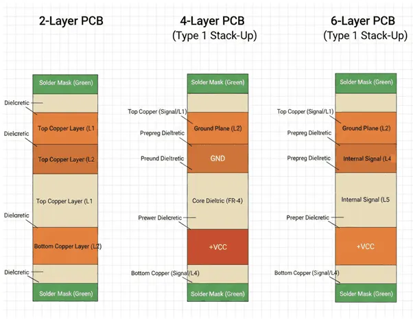
RF laminate PCB stack-up refers to the layered arrangement of conductive traces, dielectric materials, and reference planes in a printed circuit board tailored for radio frequency applications. These stack-ups use specialized low-loss laminates with stable dielectric constants and low dissipation factors to support signals from hundreds of megahertz to tens of gigahertz. Signal integrity depends on precise control of transmission line characteristics within this structure. In high-frequency environments, mismatches in RF PCB stackup impedance cause reflections that distort waveforms and reduce system efficiency. Controlled impedance RF PCB designs prevent these issues by maintaining consistent characteristic impedance across traces. Ultimately, a well-planned stack-up directly impacts data rates, noise margins, and compliance with performance specifications.
The relevance of stack-up design intensifies in modern applications like 5G infrastructure and satellite communications where frequencies exceed several gigahertz. Engineers face challenges from dielectric variations, via transitions, and coupling between layers that compromise signal quality. Ground plane RF PCB configurations provide return paths that stabilize impedance, while power plane RF PCB integration must avoid disrupting RF signals. Neglecting these factors results in higher bit error rates and failed prototypes. Adhering to standards like IPC-6018D for high-frequency boards ensures qualification for demanding environments. Proper stack-up planning reduces iterations during development and enhances manufacturability.
Technical Principles of RF Stack-Up Design
Transmission line theory forms the foundation of RF laminate PCB stack-up design. In microstrip configurations, a signal trace runs over a dielectric substrate backed by a ground plane, exposing part of the field to air. This setup yields a characteristic impedance influenced by trace width, dielectric thickness, and effective dielectric constant. Stripline structures embed the trace between two ground planes fully within the dielectric, offering uniform field distribution but requiring symmetric dielectrics. RF PCB stackup impedance calculations account for these geometries to achieve target values like 50 ohms single-ended or 100 ohms differential. Variations in laminate thickness or material properties directly affect impedance tolerance.
Microstrip vs stripline RF PCB choices hinge on trade-offs in shielding, loss, and fabrication. Microstrip lines radiate more energy due to the open top side, making them susceptible to crosstalk and external interference, yet they simplify component access and heat dissipation. Stripline provides superior shielding with fields confined between planes, reducing radiation and EMI, but demands precise etching and higher layer counts. Controlled impedance RF PCB requires field solvers or calculators to model these effects accurately during design. Ground planes in RF PCB stack-ups serve as low-inductance return paths, minimizing loop areas for magnetic fields. Power planes, when used, must incorporate splits or moats to isolate RF sections from digital noise.
Dielectric materials in RF laminates exhibit low dielectric constants typically below 4 and dissipation factors under 0.005 to limit signal attenuation. Stack-up symmetry prevents warpage during thermal cycling, maintaining trace-to-plane spacing. Via fences or stitching along trace edges enhance ground plane RF PCB effectiveness by providing multiple return paths. Power plane RF PCB placement adjacent to signal layers can introduce coupling if not decoupled properly. IPC-2221B outlines general design guidelines that apply to these high-frequency considerations. These principles ensure predictable propagation delays and minimal phase noise.
Related Reading: The Art of RF PCB Trace Design: Width, Spacing, and Geometry
Practical Solutions and Best Practices
Start stack-up design by defining impedance requirements based on system specifications. Allocate signal layers adjacent to continuous ground planes for tight coupling, typically 5 to 10 mils spacing depending on frequency. Symmetric build-ups with paired core and prepreg thicknesses balance mechanical stresses. For RF PCB stackup impedance control, specify tolerances like plus or minus 10 percent on fabrication drawings. Hybrid stack-ups combine RF laminates for critical layers with standard materials for others to optimize cost. Verify designs through electromagnetic simulations before committing to prototypes.
Incorporate multiple ground plane RF PCB layers to reference all signals effectively. Avoid splits under RF traces to prevent impedance discontinuities; use power planes sparingly in RF zones. Microstrip suits antennas and connectors where radiation is tolerable, while stripline excels in dense internal routing. Controlled impedance RF PCB fabrication involves test coupons on panels for TDR verification. Route high-speed traces perpendicular between layers to reduce broadside coupling. Follow IPC-2228 for sectional requirements in high-frequency designs to align with proven practices.
Layer sequencing follows rules like signal-ground-signal-ground for optimal isolation. Power plane RF PCB integration requires decoupling capacitors near vias to bypass noise. Minimize via usage with blind or buried types where possible, as they introduce stubs affecting high frequencies. Thermal management via thicker coppers or embedded heat spreaders supports power distribution without compromising RF performance. Document stack-up details including material Dk, Df, and CTE for manufacturer review. These steps yield robust designs resilient to process variations.
Related Reading: High Speed RF PCB Design: Techniques for Maintaining Signal Integrity at Gigahertz Frequencies
Troubleshooting Common Stack-Up Issues
Engineers often encounter impedance mismatches from dielectric thickness variations in RF laminate PCBs. Measure fabricated boards with time-domain reflectometry to identify deviations and correlate with stack-up models. Excessive crosstalk signals buried return path interruptions; add stitching vias to restore ground plane RF PCB integrity. Radiation from microstrip vs stripline RF PCB choices manifests as EMI failures; transition to stripline for sensitive circuits. Power plane RF PCB resonances cause unexpected losses; isolate with guard traces or grounded coplanar waveguides.
Warpage in asymmetric stack-ups alters clearances, leading to shorts or opens post-assembly. Balance layers and select matched CTE materials to mitigate. Insertion loss spikes indicate poor laminate selection; audit Df values against frequency needs. Simulate full stack-up including vias before layout finalization. These diagnostics, grounded in standards like IPC-6018D, streamline resolutions.
Conclusion
Effective RF laminate PCB stack-up design hinges on precise impedance control, strategic plane placement, and informed transmission line choices. Balancing microstrip vs stripline RF PCB benefits ensures signal integrity across frequencies. Ground plane RF PCB dominance and judicious power plane RF PCB use minimize losses and noise. Adhering to core principles and best practices reduces design risks and iterations. Electrical engineers equipped with these insights deliver high-performance boards ready for production.
FAQs
Q1: What factors most influence RF PCB stackup impedance?
A1: RF PCB stackup impedance depends on trace width, dielectric thickness, material dielectric constant, and reference plane proximity. Engineers calculate values using field solvers to hit targets like 50 ohms. Variations in prepreg or core thicknesses alter effective epsilon, demanding tight fab tolerances. Ground plane RF PCB continuity further stabilizes impedance. Controlled impedance RF PCB verification via coupons confirms design intent.
Q2: How does microstrip vs stripline RF PCB impact signal integrity?
A2: Microstrip offers easy access but higher radiation and crosstalk, suiting lower frequencies. Stripline shields better with dual planes, ideal for dense high-frequency routing despite fabrication complexity. Choose based on EMI needs and layer count. Both support controlled impedance RF PCB when spacings are optimized. Simulations predict performance differences accurately.
Q3: Why prioritize ground plane RF PCB in stack-ups?
A3: Ground plane RF PCB provides low-inductance returns, tight coupling, and shielding for traces. Continuous planes prevent discontinuities that cause reflections. Stitching vias enhance effectiveness at transitions. They form the backbone of RF PCB stackup impedance control. Splitting risks impedance jumps, so maintain solidity under signals.
Q4: When should power plane RF PCB be used in RF designs?
A4: Power plane RF PCB suits voltage distribution but requires isolation from RF paths to avoid coupling. Place away from signals or split with moats. Decouple extensively to suppress noise. In pure RF boards, dedicated supplies via traces suffice. Balance with ground plane RF PCB for integrity.
References
IPC-6018D — Qualification and Performance Specification for High-Frequency/Microwave Printed Boards. IPC
IPC-2221B — Generic Standard on Printed Board Design. IPC
IPC-2228 — Sectional Design Standard for Radio Frequency (RF) and Microwave Printed Boards. IPC


