 ALLPCB


Introduction
High-speed RF PCBs operate at gigahertz frequencies where signal integrity becomes critical for reliable performance. At these speeds, signals behave more like electromagnetic waves than simple electrical pulses, leading to challenges such as reflections, crosstalk, and attenuation. Engineers designing high-speed RF PCBs must prioritize techniques that preserve waveform fidelity across the board. Gigahertz PCB design demands precise control over materials, layout, and fabrication to minimize losses and maintain low noise. This article explores proven methods for achieving signal integrity in high-speed RF PCB applications, drawing on established engineering principles. By understanding these techniques, designers can optimize performance for demanding RF systems.
Understanding Signal Integrity in High-Speed RF PCBs
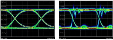
Signal integrity refers to the ability of an electrical signal to maintain its intended shape and timing from source to receiver. In high-speed RF PCBs, degradation occurs due to impedance mismatches, dielectric losses, and electromagnetic interference at gigahertz frequencies. Poor signal integrity high-speed PCB results in bit errors, reduced data rates, and system failures in applications like wireless communications and radar. Factors such as conductor surface roughness and substrate absorption exacerbate issues as frequencies climb into the multi-gigahertz range. Engineers must analyze these effects using time-domain reflectometry and vector network analysis to quantify integrity. Addressing signal integrity early in the design phase ensures compliance with performance specifications.
Why Signal Integrity Matters in Gigahertz PCB Design
Gigahertz PCB design pushes the limits of traditional PCB fabrication, where wavelengths shorten to millimeters, making board dimensions comparable to signal periods. This proximity amplifies parasitic effects, turning minor layout flaws into major performance killers. In RF systems, maintaining signal integrity high-speed PCB directly impacts metrics like return loss, insertion loss, and noise figure. For instance, excessive attenuation at 10 GHz can halve effective range in transceivers. Industry demands for 5G, mmWave, and phased arrays heighten the need for robust designs. Neglecting these principles leads to costly respins and delays in product deployment.
Core Technical Principles for Signal Integrity at Gigahertz Frequencies
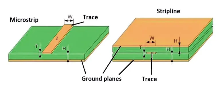
At gigahertz frequencies, transmission lines dominate signal propagation in high-speed RF PCBs. Microstrip, stripline, and coplanar waveguide configurations each offer unique impedance and loss profiles suited to specific needs. Skin effect confines currents to conductor surfaces, increasing effective resistance and ohmic losses proportional to the square root of frequency. Dielectric losses, governed by the material's dissipation factor, become dominant above 5 GHz, converting signal energy to heat. Radiation losses occur when traces act as unintentional antennas due to discontinuities. Understanding these principles allows engineers to model and predict behavior accurately.
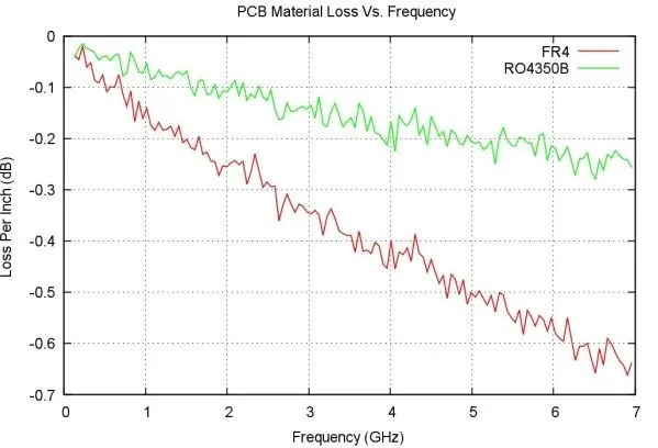
RF PCB material high-speed selection hinges on low dielectric constant (Dk) and low dissipation factor (Df) to minimize velocity and attenuation. Materials with stable Dk over frequency and temperature prevent timing skew in multi-layer stacks. Conductor losses scale with surface roughness, where RMS values below 1 micron reduce skin effect penalties. Reference planes provide return paths, but gaps introduce inductance that degrades integrity. Coupling between adjacent traces generates crosstalk, modeled as capacitive and inductive near-end/far-end effects. Balancing these elements ensures predictable signal behavior.
RF PCB Design Rules for High-Speed Signal Integrity
RF PCB design rules high-speed emphasize 50-ohm or 75-ohm controlled impedance for most RF lines. Trace width and spacing must account for manufacturing tolerances, typically holding impedance within 10% variation. Minimum via spacing exceeds three times the board thickness to curb coupling. Ground stitching vias placed every quarter-wavelength along reference planes suppress cavity resonances. Bend radii should exceed five times trace width to avoid mode conversion in curved sections. Adhering to these rules, as outlined in IPC-2221B, prevents common pitfalls in high-speed RF PCB layouts.
Layer stackup defines the foundation for signal integrity high-speed PCB. Symmetric builds with thin dielectrics between signal and ground layers reduce loop inductance. Core and prepreg thicknesses dictate characteristic impedance, requiring precise modeling. Vias transitioning layers introduce stubs that reflect signals unless backdrilled or tuned. Power planes should interleave with ground planes using extensive stitching. This configuration minimizes simultaneous switching noise and provides low-impedance return paths.
Material Selection Strategies for Gigahertz PCB Design
RF PCB material high-speed choices prioritize hydrocarbons, PTFE blends, or ceramics with Df below 0.005 at 10 GHz. Low Dk values around 3.0 ensure faster signal speeds and compact layouts. Thermal stability prevents Dk drift during operation, crucial for phased-locked loops. Coefficient of thermal expansion matching between layers avoids warpage under reflow. Moisture absorption must stay under 0.1% to prevent performance shifts. These properties directly influence insertion loss budgets in gigahertz PCB design.
Optimizing Vias and Transitions in High-Speed RF PCBs
Vias represent major discontinuities in high-speed RF PCBs, with stub lengths creating resonant nulls. Backdrilling removes unused via portions, reducing stubs to under 0.5 mm for 10 GHz operation. Blind or buried vias limit penetration, preserving reference plane integrity. Transition zones from microstrip to stripline require tapered sections or radial stubs for broadband matching. Ground vias encircling signal vias form coax-like structures, minimizing radiation. These techniques maintain return loss below -20 dB across bands.
Advanced Routing Techniques for Gigahertz Frequencies
Routing in gigahertz PCB design demands length-matched pairs for differential signals to balance skew. Serpentine patterns equalize paths without introducing excessive loss. Avoid 90-degree bends; use 45-degree miters or curves to preserve polarization. Density rules limit trace-to-trace spacing to three times dielectric thickness. Meander sections for clock lines incorporate shielding traces grounded on both sides. Compliance with IPC-6018C ensures fabrication feasibility for these fine features.
Power and Ground Integrity Considerations
Power distribution networks in high-speed RF PCBs require decoupling capacitors placed within 1 mm of IC pins. Multi-layer ceramic types with low ESL handle gigahertz harmonics. Solid ground planes, split only at DC blocks, provide uniform return currents. Via fences along board edges contain EMI. PDN impedance targets below 10 milliohms up to 10 GHz. These strategies couple power integrity with signal paths effectively.
Verification and Testing Best Practices
Simulation precedes fabrication, using 3D electromagnetic solvers for S-parameter extraction. Fabricated prototypes undergo TDR for impedance profiles and VNA for loss characterization. Fixture de-embedding corrects measurement errors from test structures. Thermal cycling verifies material stability per IPC-6012DS. Field testing with spectrum analyzers confirms radiated emissions. Iterative refinement based on these validates signal integrity high-speed PCB.
Troubleshooting Signal Integrity Issues
Common failures include unexpected resonances from unterminated stubs. Eye diagram closure signals excessive jitter or loss. Crosstalk spikes indicate inadequate spacing. Use probing to isolate issues, then adjust stackup or reroute. Material inconsistencies cause frequency-dependent attenuation. Systematic diagnosis restores performance.
Conclusion
High-speed RF PCB design thrives on meticulous attention to signal integrity at gigahertz frequencies. Key techniques like controlled impedance, low-loss materials, optimized vias, and precise routing form the backbone of reliable systems. RF PCB design rules high-speed, grounded in standards like IPC-2221B, IPC-6018C, and IPC-6012DS, guide engineers toward success. Integrating power integrity and thorough verification minimizes risks. Designers adopting these practices achieve superior performance in demanding RF applications. Future advancements will build on these foundations for even higher frequencies.
FAQs
Q1: What are the primary challenges in gigahertz PCB design for signal integrity?
A1: Gigahertz PCB design faces attenuation from dielectric and conductor losses, reflections from mismatches, and crosstalk between traces. Engineers counter these with low Df RF PCB material high-speed and controlled impedance routing. Proper stackup and via optimization further preserve waveforms. Testing verifies compliance across the band.
Q2: How do RF PCB design rules high-speed differ from standard PCBs?
A2: RF PCB design rules high-speed enforce tighter tolerances on impedance, spacing, and surface finish to combat skin effect and radiation. Trace bends use miters, and stitching vias prevent resonances. Standards like IPC-2221B specify these for high-frequency performance. This contrasts with digital boards focused on DDR timing.
Q3: Why is RF PCB material high-speed critical for signal integrity high-speed PCB?
A3: RF PCB material high-speed with low Dk and Df reduces phase velocity errors and energy dissipation at gigahertz frequencies. Stable properties prevent thermal-induced shifts. Matching CTE avoids mechanical stress. Selection directly impacts insertion loss budgets in high-speed RF PCB.
Q4: What verification methods ensure signal integrity in high-speed RF PCBs?
A4: Use TDR for impedance, VNA for S-parameters, and eye diagrams for overall quality. Simulate PDN impedance and EMI. Per IPC-6018C, qualify boards for microwave use. Prototype testing identifies fabrication variances early.
References
IPC-2221B — Generic Standard on Printed Board Design. IPC, 2012
IPC-6012DS — Qualification and Performance Specification for Double-Sided Rigid Printed Boards. IPC, 2015
IPC-6018C — Qualification and Performance Specification for High Frequency (Microwave) Printed Boards. IPC, 2017





