ALLPCB


Introduction
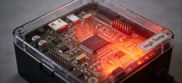
Printed circuit boards (PCBs) power everything from consumer electronics to industrial controls, but rising power densities demand effective thermal management. Without proper heat dissipation, components overheat, leading to performance degradation, reliability issues, and outright failures. Engineers face a balancing act: implementing robust thermal solutions while controlling costs in PCB thermal management. This article delves into budget considerations for PCB thermal management cost, exploring trade-offs between basic and advanced approaches. From passive heat sinks to active cooling fans, understanding these elements helps optimize designs for both performance and economics. Key factors like material choices and layout strategies play pivotal roles in achieving cost-effective design without compromising functionality.
Understanding PCB Thermal Management and Its Importance
PCB thermal management involves strategies to dissipate heat generated by active components, traces, and power planes. Heat arises primarily from electrical resistance in conductors and power dissipation in semiconductors, accumulating if not addressed. In high-reliability applications, poor thermal control accelerates electromigration, solder joint fatigue, and dielectric breakdown. Industry standards such as IPC-2221 underscore the need for thermal analysis during design to predict hotspots and ensure board longevity. For electric engineers, neglecting this aspect inflates long-term costs through field failures and rework. Ultimately, effective thermal management safeguards performance margins while aligning with project budgets.
As power levels climb in modern designs, thermal solutions become non-negotiable. Compact form factors exacerbate challenges, concentrating heat in limited spaces. Budget decisions hinge on distinguishing essential dissipation from over-engineering, preventing unnecessary expenses. Engineers must evaluate operating environments, from ambient air to forced convection, to select appropriate methods.
Core Principles of Heat Dissipation in PCBs
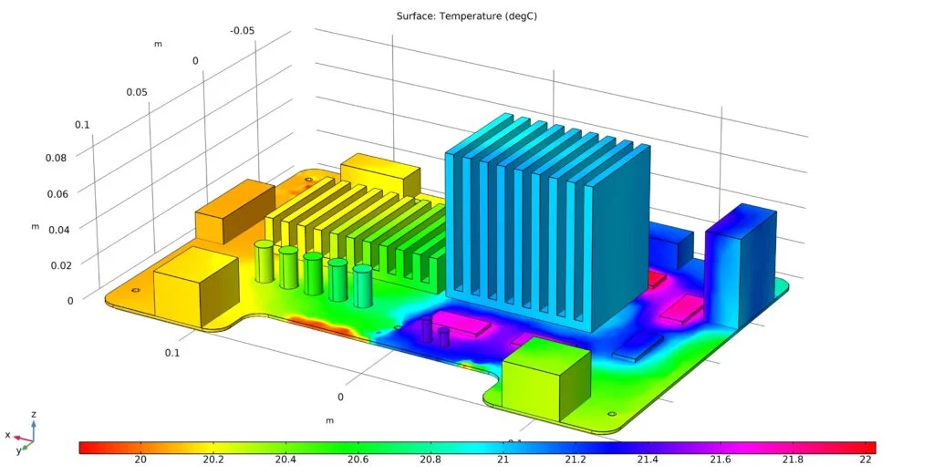
Heat transfer in PCBs relies on conduction through materials, convection to surrounding air, and radiation, though the latter contributes minimally at typical temperatures. Conduction dominates within the board, governed by thermal conductivity values of copper (high) versus FR-4 substrates (low). Thermal resistance, measured in degrees Celsius per watt, quantifies a path's effectiveness; lower values indicate better dissipation. Engineers model these using finite element analysis, factoring in via placement and plane thickness. IPC-2152 provides guidelines for current-carrying capacity, linking trace width to temperature rise and thus thermal demands.
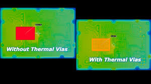
Thermal vias bridge layers, channeling heat from inner planes to surface pads efficiently. Arrays of vias under hotspots reduce resistance but add fabrication complexity and cost. Copper thickness influences conduction; heavier pours enhance spreading but increase material expenses. Surface finishes and solder masks also affect emissivity for radiation. Convection depends on airflow, board orientation, and enclosure design, requiring simulation for accuracy.
Radiation plays a secondary role, proportional to the fourth power of absolute temperature per Stefan-Boltzmann law, but practical designs prioritize conduction and convection. Understanding these mechanisms allows engineers to prioritize budget allocations toward high-impact features.
Related Reading: Thermal Vias in PCB Design: The Complete 2025 Guide to Efficient Heat Dissipation
Budget Factors in Passive Thermal Solutions
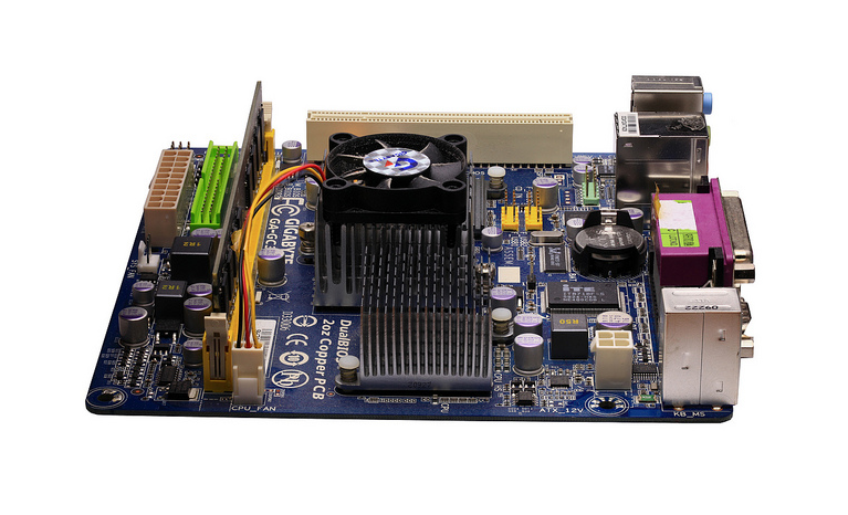
Passive thermal solutions form the foundation of cost-effective design, avoiding power-hungry active components. Heat sinks attach to high-power devices, extending surface area for convection; aluminum extrusions offer good value due to machinability and thermal properties. Fin density, height, and base thickness determine performance versus weight and attachment costs. Engineers select profiles balancing airflow impedance with dissipation needs, often using empirical charts for estimation.
Thermal vias represent a low-cost, board-integrated option. Drilling and plating vias adds steps, yet microvias in high-density interconnects (HDI) designs justify expenses through multilayer efficiency. Filling vias with conductive epoxy boosts conductivity but elevates costs. Placement density under chips optimizes paths to outer layers, minimizing temperature gradients.
Advanced materials shift budgets toward premium laminates with enhanced thermal conductivity, like ceramic-filled epoxies. These outperform standard FR-4 in spreading heat horizontally, reducing reliance on external sinks. However, higher sheet costs and processing sensitivities demand volume justification. Metal-core boards, with aluminum substrates, excel in LED lighting but introduce mechanical challenges like CTE mismatch.
Copper planes and balanced stacking sequences distribute heat evenly, a no-added-cost strategy if planned early. Thicker foils (2-3 oz) improve conduction but raise etching expenses and signal integrity concerns. Engineers weigh these against via fields or embedded coins for extreme cases.
Active Cooling and Hybrid Approaches
Cooling fans introduce forced convection, dramatically lowering thermal resistance at the expense of power draw and noise. Axial blowers suit enclosures, while radial fans handle localized hotspots. Budgets must account for mounting hardware, cabling, and lifespan; fans fail over time, necessitating redundancy in critical systems. Variable-speed controllers optimize energy use but add electronics costs.
Hybrid systems combine passives with actives for versatility. For instance, heat sinks paired with low-profile fans handle transient peaks economically. Vapor chambers or heat pipes, embedded or attached, offer high-capacity spreading for compact designs, though fabrication premiums apply. JEDEC standards like JESD51 guide thermal characterization, ensuring comparable metrics across solutions.
Procurement teams evaluate total cost of ownership: initial outlay plus maintenance and energy. Active solutions shine in variable loads but falter in sealed or vibration-prone environments.
Cost-Effective Design Strategies for Thermal Management
Achieving cost-effective design starts with upfront simulation to avoid iterations. Tools model airflow and conduction iteratively, identifying vias or plane cutouts early. Layer count minimization reduces material while enabling buried power planes for heat spreading.
Component selection influences budgets profoundly; low-thermal-resistance packages (e.g., QFN with exposed pads) integrate dissipation natively. Grouping heat sources facilitates shared sinks, cutting part counts. Board size optimization via panelization amortizes setup costs across multiples.
Material trade-offs prioritize copper content over exotic fillers unless densities demand it. Standard 1 oz copper with dense thermal vias often suffices, per IPC-2221 design curves. Enclosure integration, like chassis conduction, leverages system-level cooling without board extras.
Fabrication partnerships streamline via-in-pad or blind vias, distributing costs. Assembly considerations, such as underfill for BGA heat paths, prevent post-process add-ons.
Testing validates budgets: infrared thermography spots issues pre-production, averting recalls. JEDEC JESD51 series standardizes junction-to-ambient metrics, aiding supplier comparisons.
Related Reading: Beginner's Guide to Thermal Pads: Simple Steps for Effective Heat Dissipation
Balancing Performance and Budget in Real-World Scenarios
Electric engineers often face trade-offs in power electronics, where MOSFETs generate kilowatts of heat. A cost-effective design might employ thermal vias under dies, augmented by a low-profile heat sink, avoiding fans for silent operation. In contrast, telecom boards prioritize advanced materials to maintain density without airflow.
Automotive applications demand robustness under vibration, favoring rugged heat sinks over delicate pipes. Budget audits reveal that 20-30% of thermal spend ties to materials, with vias adding 10-15% in multilayer boards, though these prevent failures costing exponentially more. Simulation-driven choices ensure compliance without excess.
Sustainability angles emerge: efficient dissipation cuts operational power, aligning with ISO 14001 environmental goals, though not directly thermal-focused.
Conclusion
PCB thermal management cost hinges on strategic choices across heat sinks, cooling fans, advanced materials, thermal vias, and layout ingenuity. Passive solutions offer baseline economics, while hybrids scale for demanding loads. Adhering to standards like IPC-2221 and IPC-2152 ensures reliability without overbudgeting. Engineers achieve cost-effective design by simulating early, selecting components wisely, and integrating system-level cooling. Prioritizing total ownership over upfront savings yields optimal outcomes. As designs evolve, these principles remain key to "cool" performance on budget.
FAQs
Q1: What factors most influence PCB thermal management cost?
A1: Material selection, such as advanced high-conductivity laminates, drives up initial expenses but can lower overall thermal solutions needs. Fabrication features like thermal vias add drilling and plating costs, while heat sinks and cooling fans introduce assembly and sourcing premiums. Design complexity, including layer count and via density, impacts tooling. Engineers balance these against reliability gains for cost-effective design. Simulations help predict hotspots without trial-and-error expenses.
Q2: How do thermal vias contribute to cost-effective PCB thermal management?
A2: Thermal vias provide efficient vertical heat paths at modest added cost, connecting inner planes to surfaces for convection. Optimal arrays under hotspots reduce thermal resistance without external parts. Plated through-holes suit most designs, while filled variants enhance performance in dense boards. Early placement in stackups avoids redesigns. Per IPC-2152 guidelines, they support higher currents, minimizing trace upsizing.
Q3: When should engineers consider advanced materials for thermal solutions?
A3: Advanced materials shine in high-power-density boards where FR-4 limits spreading. Ceramic or metal-filled epoxies offer superior in-plane conductivity, reducing heat sink sizes. Costs justify in volume production or harsh environments. They integrate seamlessly with thermal vias for holistic management. JEDEC JESD51 aids performance benchmarking. Standard materials suffice for moderate loads, preserving budgets.
Q4: What role do heat sinks and cooling fans play in budgeting?
A4: Heat sinks deliver passive dissipation economically via extended surfaces, with aluminum providing value. Cooling fans boost convection for peaks but add power and maintenance costs. Hybrids optimize for variable loads. Attachment methods like clips or epoxy influence expenses. System airflow analysis ensures sizing avoids overspend. Cost-effective design pairs them judiciously with board-level features.
References
IPC-2221B — Generic Standard on Printed Board Design. IPC, 2012
IPC-2152B — Standard for Determining Current Carrying Capacity in Printed Board Trace. IPC, 2023
JEDEC JESD51-14 — Transient Dual Interface Test Method for the Measurement of the Thermal Resistance Junction-to-Case of Semiconductor Devices with Heat Sink. JEDEC, 2010