 ALLPCB


Introduction
In modern PCB assembly, achieving precise solder paste deposition is crucial for high-density surface mount technology applications. Step stencils, also known as multi-level stencils, address the challenges of mixed component sizes on a single board by varying stencil thickness across different apertures. This step stencil design enables better solder paste volume control, reducing defects like bridging or insufficient solder joints in complex assemblies. Electric engineers often encounter scenarios where standard uniform-thickness stencils fall short, especially with fine-pitch devices alongside larger components. By exploring multi-level aperture design, this article provides practical insights into optimizing SMT stencil performance for reliable PCB assembly outcomes. Understanding these principles helps troubleshoot printing issues and enhances overall process yield.
What Are Step Stencils and Why Do They Matter in PCB Assembly?
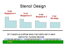
Step stencils feature regions of different thicknesses within the same stencil, allowing tailored solder paste heights for diverse component types. Typically, thinner sections serve fine-pitch components like 01005 resistors or 0.3mm pitch BGAs, while thicker areas accommodate larger pads for QFNs or connectors. This multi-level approach contrasts with traditional single-thickness SMT stencils, which compromise paste volume across the board. In complex PCB assemblies, inconsistent paste volumes lead to reflow defects, such as tombstoning or open joints, making step stencil design essential for high-reliability electronics. Engineers benefit from this technology in high-mix, low-volume production where component diversity is common. Ultimately, step stencils improve first-pass yield by matching paste volume to land pattern requirements.
The relevance grows with shrinking component sizes and denser boards, where solder paste volume control directly impacts joint integrity. Without multi-level stencils, assemblers might resort to multiple printing passes or manual adjustments, increasing cycle time and error risk. IPC-7525 guidelines emphasize step stencils for scenarios where a single thickness cannot meet all aperture needs. This design flexibility supports advanced packaging like SiP modules and supports automotive or medical-grade PCB assembly demands.
Related Reading: Step Stencils: Optimizing Solder Paste Deposition for Mixed Component PCBs
The Technical Principles Behind Multi-Level Aperture Design
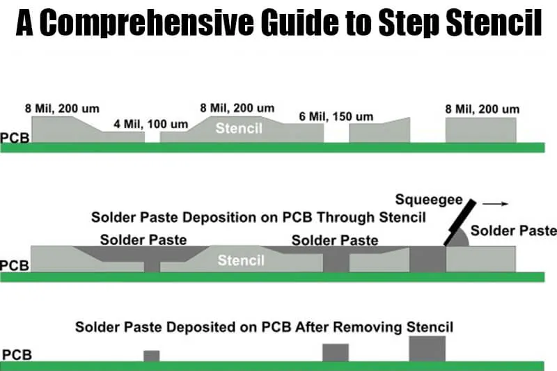
Multi-level aperture design relies on precise control of stencil thickness to dictate solder paste brick height and volume. Thinner apertures, often 0.1mm or less, deposit minimal paste for fine-pitch devices to prevent bridging during reflow. Thicker regions, up to 0.15mm, provide ample volume for larger components requiring robust fillet formation. The step transition creates a controlled shear during printing, ensuring clean release and consistent transfer efficiency. Area ratio, defined as (aperture area / aperture perimeter x thickness), must exceed 0.66 per IPC-7525 to optimize paste release. Poor ratios lead to insufficient transfer, causing voids or starvation in joints.
Step-down configurations dominate, where the base stencil is thick, and localized thinning occurs over fine-pitch zones. Step-up designs add material for selective thickening, useful when base material is thin overall. Multi-level stencils extend this to three or more levels, handling ultra-complex boards with micro-BGAs and discrete passives simultaneously. Alignment tolerances tighten at steps, typically under 25 microns, to avoid paste smearing. These principles ensure solder paste volume control aligns with component standoff and land geometry.
Key Design Considerations for Step Stencil Design
Effective step stencil design starts with analyzing the bill of materials and land patterns to determine optimal thicknesses per aperture group. Group similar components to minimize step count, as each level increases fabrication complexity and cost. Maintain a minimum step height of 50 microns to ensure structural integrity during printing pressure. IPC-7525 recommends keep-out zones around steps, at least 0.89mm per 0.025mm thickness difference, to prevent paste bleed. Aperture shapes influence release: trapezoidal or U-shaped walls reduce entrapment compared to rectangular cuts.
Wall finish quality affects transfer efficiency, with polished or nano-coated surfaces enhancing clean wipe-off. Framed stencils suit high-volume runs, while frameless fit universal printers. Fiducials on the stencil match PCB marks for subpixel alignment, critical in multi-level setups. Simulate paste volume using software to verify against J-STD-001 soldering criteria before fabrication. Balancing these factors yields robust step stencil design for demanding PCB assembly.
Fabrication Methods for Step Stencils
Laser cutting dominates step stencil production due to its precision in creating sharp step edges and complex apertures. High-power YAG or fiber lasers ablate foil material layer by layer, achieving tolerances under 5 microns. This method suits nickel or stainless steel foils from 0.076mm to 0.152mm thick. Chemical etching offers cost-effective alternatives for simpler steps but risks undercutting at transitions. Electroforming builds stencils atom-by-atom on mandrels for superior wall profiles, ideal for ultra-fine pitch though costlier.
Hybrid approaches combine laser-cut base with welded thicker sections for step-up designs. Post-processing like electropolishing refines surfaces for better paste release. Fabrication must adhere to material flatness specs to avoid warpage under squeegee pressure. Each method impacts durability, with laser-cut stencils lasting 50,000+ prints in production.
Best Practices for Solder Paste Volume Control and Implementation
Select stencil thickness based on smallest pitch: 1:1 pitch-to-thickness ratio for fine features, scaling up for coarser ones. Validate volume targets via SPI metrology, aiming for 100-130% transfer efficiency. Optimize printing parameters: squeegee speed 20-50mm/s, pressure 2-5kg, snap-off 1-2mm. Use type-4 or finer paste for step stencils to minimize viscosity issues at transitions. Clean stencil every 5-10 prints with optimized chemistry to prevent residue buildup.
In PCB assembly, qualify step stencils with AOI and X-ray post-print to correlate volume with reflow performance. Adjust for board warpage by compensating stencil flatness. Document process windows per IPC-7525 to support yield analysis. These practices ensure solder paste volume control translates to defect-free joints.
Related Reading: The Ultimate Guide to Step Stencil Manufacturing: Processes and Materials
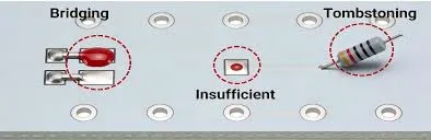
Troubleshooting Common Issues with Step Stencils
Insufficient paste on thick areas often stems from poor squeegee contact over steps; increase pressure or add ramps. Bridging in thin zones indicates excessive volume or misalignment; refine aperture size or alignment. Step cracking arises from over-stressing during fabrication; limit step height and use ductile foils. Paste smearing at transitions requires wider keep-out or smoother walls via polishing.
Inspect for foreign object debris pre-print, as it amplifies defects in multi-level designs. If yields drop, cross-section samples to measure actual volumes against design. Correlate with reflow profiles per J-STD-001 to isolate stencil versus process issues. Systematic troubleshooting restores reliability in SMT stencil applications.
Conclusion
Step stencils revolutionize multi-level aperture design for complex PCB assemblies by enabling precise solder paste volume control. Engineers gain flexibility to handle diverse components without compromising quality. Adhering to guidelines like IPC-7525 ensures robust implementation and troubleshooting success. As densities rise, mastering step stencil design becomes indispensable for efficient SMT processes. Prioritize simulation, validation, and process control for optimal results.
FAQs
Q1: What is the primary benefit of step stencil design in PCB assembly?
A1: Step stencil design provides targeted solder paste volume control for mixed component sizes, preventing defects like insufficient solder or bridging. Thinner areas suit fine-pitch parts, while thicker zones support larger pads. This multi-level stencil approach boosts first-pass yields in high-density boards. Follow IPC-7525 for optimal thickness ratios.
Q2: How does multi-level stencil fabrication impact SMT stencil performance?
A2: Laser cutting ensures precise step edges in multi-level stencils, enhancing paste release and alignment. Etching or electroforming offers alternatives based on volume needs. Proper wall finishes minimize entrapment during printing. Troubleshoot by measuring transfer efficiency post-fabrication.
Q3: Why is solder paste volume control critical with step stencils?
A3: Solder paste volume control matches deposit height to land patterns, ensuring reliable reflow joints per J-STD-001. Inconsistent volumes cause tombstoning or voids in PCB assembly. Simulate apertures to hit 100-130% efficiency targets. Adjust printing parameters for consistent results.
Q4: When should electric engineers choose a step stencil over a standard SMT stencil?
A4: Opt for step stencils in complex assemblies with fine-pitch and large components on one board. Standard SMT stencils fail volume control here, risking defects. Multi-level designs handle this efficiently. Validate with SPI for production readiness.
References
IPC-7525B - Stencil Design Guidelines. IPC, 2011
IPC-7525C - Stencil Design Guidelines. IPC
J-STD-001 - Requirements for Soldered Electrical and Electronic Assemblies. IPC, latest revision


