 ALLPCB


Introduction
Stencil printing plays a critical role in the surface mount technology assembly process for prototype printed circuit boards. Electrical engineers rely on this method to apply solder paste precisely onto pads before component placement, enabling reliable reflow soldering. In prototype development, where iterations happen frequently, prototype PCB stencil printing stands out for its ability to support quick turnaround times. Rapid stencil fabrication techniques allow teams to produce stencils from digital design files in hours rather than days, accelerating the overall prototyping cycle.
This flexibility proves essential when troubleshooting design issues, such as inadequate paste volume or bridging risks. Engineers can implement stencil printing design changes swiftly by modifying aperture patterns in their layout software and regenerating the stencil file. Such adaptability minimizes downtime during validation phases, ensuring prototypes align closely with performance requirements. By mastering these aspects, teams achieve higher first-pass yields and faster time-to-market for new electronics projects.
What Is Stencil Printing for Prototype PCBs and Why It Matters
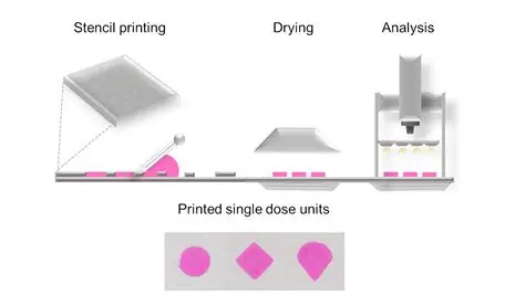
Stencil printing involves depositing solder paste through a thin metal or polymer sheet with precisely cut apertures aligned to PCB pads. For prototypes, the stencil acts as a template that transfers paste in exact volumes, preparing the board for pick-and-place and reflow operations. This process replaces manual paste application, which proves inconsistent and time-consuming for small runs. Prototype PCB stencil printing thus ensures uniform paste height and area coverage, critical for forming strong solder joints under thermal stress.
The relevance grows in fast-paced engineering environments where design revisions occur multiple times. Without efficient stencil methods, delays in paste application slow down assembly testing and debugging. Rapid stencil fabrication addresses this by enabling on-demand production, often within the same day as file submission. Engineers benefit from reduced assembly defects, such as insufficient solder or tombstoning, which stem from poor paste deposition.
Moreover, this technique supports diverse prototype complexities, from fine-pitch components to mixed-technology boards. It aligns with industry needs for reliability in early-stage validation, where electrical performance must match simulation results. Ultimately, stencil printing empowers engineers to focus on functionality rather than fabrication hurdles.
Technical Principles Behind Rapid Stencil Fabrication
Rapid stencil fabrication primarily uses laser cutting on stainless steel foils, offering precision and speed over traditional chemical etching. Laser systems vaporize material to form apertures with smooth walls, minimizing paste release issues like sticking. This direct-from-data approach bypasses photomask steps, cutting lead times to under 24 hours for standard prototypes. Foil thickness typically balances aperture size and paste volume needs, influencing transfer efficiency during printing.
Aperture design follows guidelines in IPC-7525C, which emphasize aspect ratios and step-down features for optimal paste rollover. Engineers adjust openings based on pad geometry to prevent bridging on adjacent pads or starving inner joints. For prototypes, frameless stencils stretch onto printer frames, eliminating fixed-frame setup delays and storage costs. This modularity suits variable board sizes common in early development.
Laser-cut edges reduce burrs compared to etched stencils, enhancing clean snap-off during printing. Surface treatments, like electropolishing, further improve paste release by creating nano-coatings on walls. These principles ensure consistent deposition across high-density layouts, vital for prototype reliability testing.
Strategies for Quick Turnaround in Prototype PCB Stencil Printing
Achieving quick turnaround starts with streamlined digital workflows from design to fabrication. Engineers export Gerber files with fiducials and apertures directly to stencil makers, avoiding format conversions that cause errors. Automated laser plotters process these files rapidly, producing stencils ready for immediate printer loading. Pairing this with high-speed printers equipped for frameless stencils completes paste application in minutes per board.
Printer setup optimization further accelerates the process. Proper tensioning of frameless stencils prevents misalignment, while automated vision systems confirm registration before printing multiple prototypes in sequence. Solder paste selection influences speed too, as type 4 or finer particles flow better through small apertures without frequent cleaning. Engineers troubleshoot slowdowns by monitoring squeegee pressure and speed, adjusting to maintain throughput without defects.
Integration with in-house assembly lines enhances overall turnaround. For instance, printing stations adjacent to reflow ovens minimize handling time. This end-to-end efficiency allows prototype iterations within a single shift, critical for time-sensitive projects.
Leveraging Design Flexibility Through Stencil Printing Design Changes
Stencil printing excels in handling design changes, a common prototype scenario when signal integrity issues or component swaps arise. Modifying aperture sizes or shapes in the design file regenerates the stencil quickly via laser methods, unlike recutting etched versions. This flexibility lets engineers experiment with paste volumes to resolve reflow problems, such as opens on BGA balls or excess on QFNs.
Rapid stencil fabrication supports A/B testing by producing variant stencils from branched design files. For example, increasing aperture area by a calculated percentage can address cold joints without respinning the entire PCB. Fiducial marks remain consistent across revisions, easing printer alignment for comparative assemblies. Such adaptability reduces engineering hours spent on manual workarounds.
Troubleshooting paste-related defects becomes iterative and data-driven. Engineers print, inspect with SPI tools, then tweak designs for the next stencil run. This cycle fosters innovation in compact layouts, where space constraints demand precise stencil printing design changes.
Related Reading: Understanding Stencil Printing: A Comprehensive Guide for SMT Assembly
Best Practices and Troubleshooting for Reliable Prototype Assemblies
Adhere to established printing parameters to maximize stencil performance in prototypes. Maintain squeegee speed between 20 to 100 mm per second, depending on paste viscosity, to ensure even rollout without smearing. Clean stencils after every 5 to 10 prints using automated wipe sequences, preventing residue buildup that causes inconsistent transfer. Alignment tolerances under 25 microns prevent offset defects, verifiable via optical fiducials.
For troubleshooting, examine common failures systematically. Insufficient paste volume often traces to low aspect ratios, addressed by referencing IPC-7525C guidelines for aperture scaling. Bridging indicates excessive paste or poor snap-off, remedied by thinner foils or wall treatments. Inspect post-print height variation with laser profilometers to correlate with reflow outcomes.
Paste storage and handling merit attention too. Condition paste at room temperature before use, kneading to homogenize particles. J-STD-001 provides criteria for joint acceptability post-reflow, guiding stencil refinements. Document changes in a revision log to track improvements across prototype builds.
Incorporate IPC-7527 principles for solder paste printing processes, focusing on equipment calibration and environmental controls like humidity below 60%. These practices yield robust prototypes ready for functional testing.
Troubleshooting Insights from Real-World Prototype Scenarios
Consider a scenario where fine-pitch QFN components exhibit tombstoning after reflow. Engineers identify uneven paste heights from stencil misalignment, correct by enhancing fiducial contrast in the design, and order a rapid stencil fabrication. The updated stencil, with adjusted squeegee paths, resolves the issue in the next run, validating the fix without full re-prototyping.
Another frequent challenge involves BGA underfill preparation, where stencil printing design changes enlarge shadow apertures for better paste containment. Troubleshooting reveals over-etching risks in laser paths, mitigated by specifying higher power settings during fabrication. Post-inspection confirms uniform deposits, proceeding to assembly.
These insights highlight proactive stencil management. Engineers log defect Pareto charts to prioritize aperture tweaks, ensuring stencil printing evolves with design maturity.
Related Reading: DIY Stencil Printing: Creating Custom Stencils for Your Electronics Projects
Conclusion
Prototype PCB stencil printing delivers unmatched quick turnaround and design flexibility for electrical engineers navigating iterative development. Rapid stencil fabrication via laser methods, combined with precise aperture design per industry standards, streamlines paste application and defect reduction. Best practices in alignment, cleaning, and troubleshooting further enhance reliability, supporting seamless transitions to production.
By embracing these techniques, teams accelerate validation cycles and refine electronics performance efficiently. Stencil printing remains a cornerstone of modern prototyping, empowering innovation without compromising quality.
FAQs
Q1: What makes prototype PCB stencil printing ideal for quick turnaround projects?
A1: Prototype PCB stencil printing leverages laser-cut frameless stencils, producible in hours from Gerber files. This bypasses slow etching, allowing immediate printer setup and paste deposition. Engineers achieve multiple assembly runs per day, troubleshooting reflow issues on-site. Combined with automated inspection, it minimizes delays in design validation cycles.
Q2: How does rapid stencil fabrication support frequent design iterations?
A2: Rapid stencil fabrication uses direct laser ablation from modified digital files, enabling stencil printing design changes without tooling delays. Engineers adjust apertures for paste volume tweaks, reprint, and test variants swiftly. This flexibility resolves bridging or starvation defects iteratively, aligning prototypes with electrical requirements efficiently. Frameless designs further speed handling.
Q3: What are common troubleshooting steps for stencil printing defects in prototypes?
A3: Start with visual and SPI inspection for paste height uniformity. Adjust squeegee pressure or speed for poor release, referencing IPC-7525C for apertures. Clean stencils frequently to avoid residue bridging. Verify alignment via fiducials, and condition paste properly. These steps, per J-STD-001 joint criteria, boost first-pass yields in rapid cycles.
Q4: Why prioritize stainless steel stencils for prototype PCB stencil printing?
A4: Stainless steel offers durability for repeated prints in prototypes, with laser-cut walls ensuring clean paste snap-off. It handles fine-pitch apertures reliably, supporting design flexibility. Electropolishing enhances release, reducing defects like insufficient solder. This material choice aligns with quick turnaround needs, outlasting polymers in iterative testing.


