 ALLPCB


Introduction
Screen printing plays a crucial role in PCB assembly, especially when applying solder paste through a stencil. For electronic hobbyists, mastering this step ensures reliable solder joints without relying on expensive equipment. Common mistakes can lead to defects like bridging or insufficient paste, ruining hours of work on prototypes. Understanding these errors helps hobbyists achieve professional results at home. This article explores frequent screen printing pitfalls and practical fixes. By avoiding them, you can improve your success rate in surface mount assembly.
What Is Screen Printing in PCB Assembly and Why It Matters
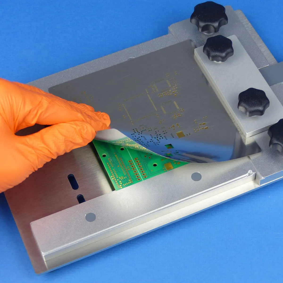
Screen printing, or stencil printing, involves spreading solder paste over a stencil aligned to the PCB pads. The paste fills the stencil openings, depositing precise amounts for component soldering. For hobbyists, this manual process replaces automated machines, making it accessible yet challenging. Poor printing causes downstream issues like weak joints or shorts during reflow. Consistent deposits are vital for fine-pitch components common in modern designs. Adhering to guidelines like those in IPC-7525C ensures quality from the start.
Common Causes of Screen Printing Mistakes
Many screen printing errors stem from basic setup oversights. Incorrect handling of the stencil or paste leads to uneven deposits. Hobbyists often rush alignment, causing paste to miss pads entirely. Pressure inconsistencies during squeegeeing exacerbate these problems. Dirty residues from previous prints build up quickly without proper care. These factors compound, turning a simple step into a frustrating bottleneck.
Applying the Wrong Squeegee Pressure
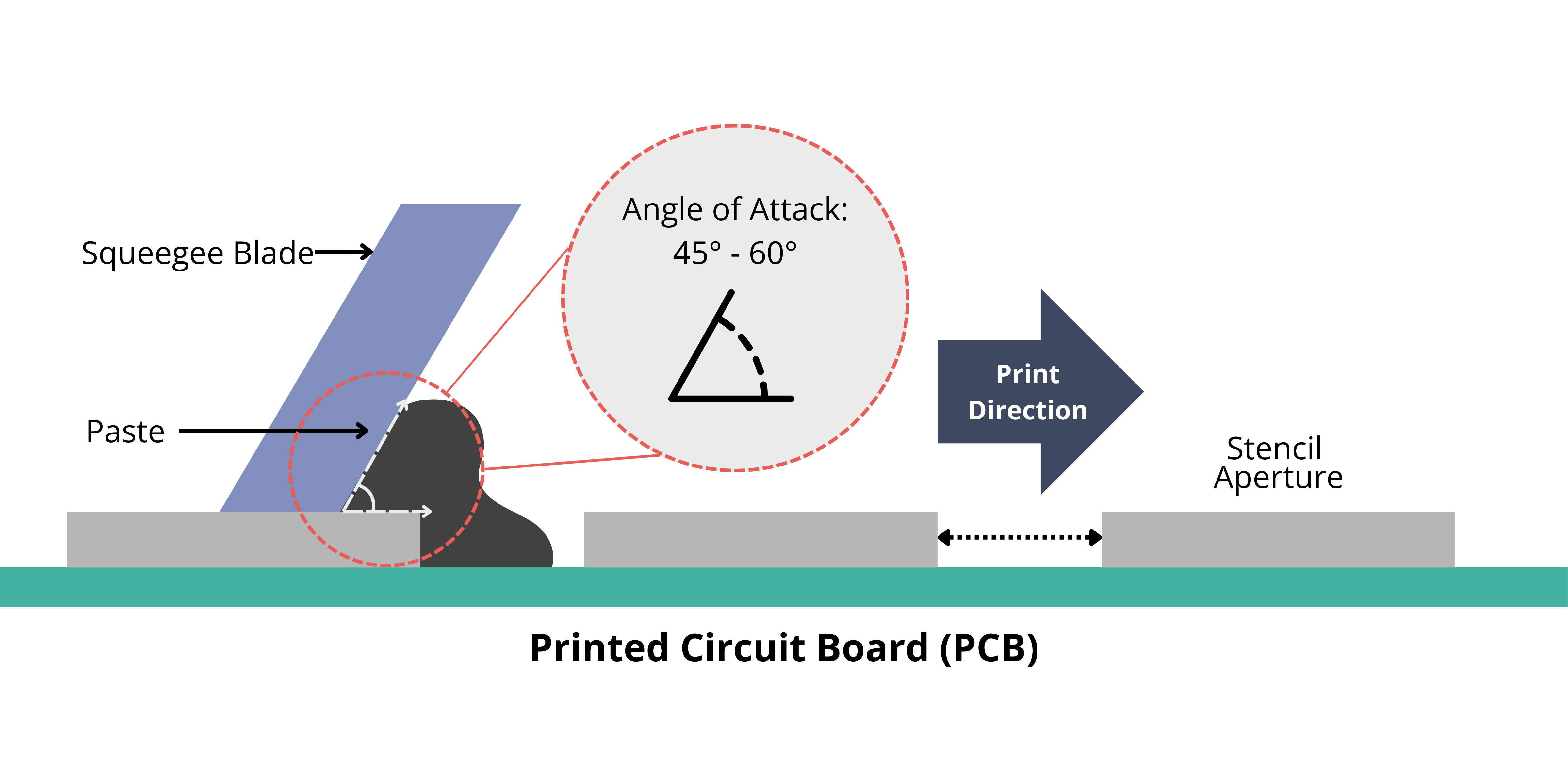
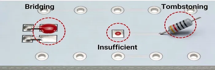
One of the most frequent mistakes is not using the right amount of pressure with the squeegee. Too much force pushes excess paste under the stencil edges, creating bridges between pads. Conversely, insufficient pressure fails to fill apertures fully, leaving starved joints. Hobbyists using manual tools must feel for even contact without overdoing it. Blade angle also interacts with pressure; a steep angle amplifies issues. Testing on scrap boards reveals the sweet spot before committing to the real PCB.
This error disrupts paste volume uniformity, as outlined in IPC-7527 for solder paste printing requirements. Uneven pressure causes streaking or skips across the board. Over time, it wears the stencil faster, compounding defects. Beginners overlook how paste viscosity changes with temperature, altering needed force. Consistent practice builds intuition for balanced application. Monitoring deposit height visually prevents most pressure-related failures.
Using Dirty or Wrinkled Materials
Using dirty or wrinkled materials ranks high among avoidable errors. Residue on the stencil bottom clogs apertures, blocking paste flow and causing incomplete transfers. Wrinkled stencils from improper storage warp apertures, leading to misalignment. Hobbyists reusing stencils without cleaning face smearing as old paste mixes with fresh. Dust or fingerprints contaminate the PCB surface, attracting more defects later. Always inspect materials under good light before starting.
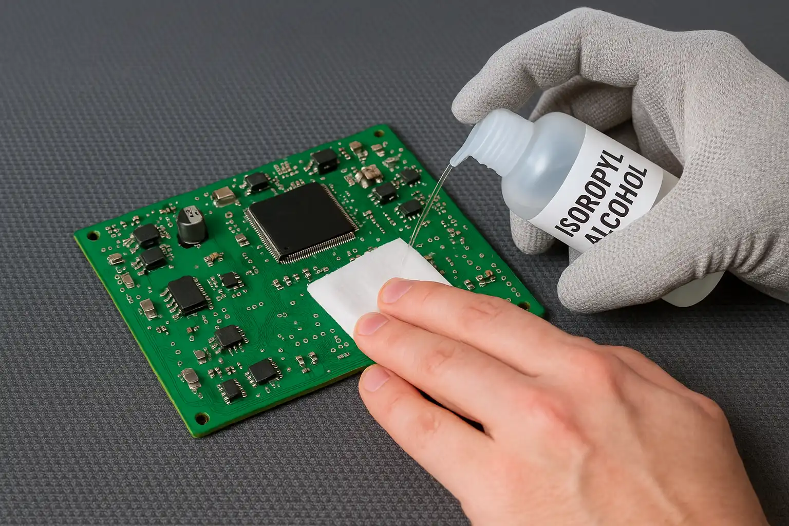
Dirt accelerates slumping, where paste spreads post-print due to poor release. Wrinkles mimic PCB warpage, shifting deposits off pads. Simple wipes with isopropyl alcohol restore cleanliness, but neglect invites bridging. Storage in flat, sealed boxes prevents wrinkles over time. Clean habits align with factory standards, boosting hobbyist yields. Regular maintenance turns potential disasters into reliable prints.
Other Key Mistakes: Alignment and Speed Issues
Poor alignment tops the list after pressure and cleanliness. Even slight offsets deposit paste incorrectly, risking tombstoning in reflow. Hobbyists must use fiducials or edges for precise setup. Excessive squeegee speed skips areas, while too slow causes smearing. Paste condition matters; expired or unmixed batches print poorly regardless of technique. PCB support prevents flexing under the stencil.
These combine destructively: misaligned dirty stencils under wrong pressure guarantee failure. Warped PCBs amplify everything, demanding flat fixtures. Hobbyists benefit from step-by-step checks before each print. Visual inspection post-print catches 80% of issues early. Patience here saves rework time.
Practical Solutions and Best Practices
Fixing screen printing starts with preparation. Select stencils matching your pitch; thinner for fine lines per IPC-7525C guidelines. Acclimate paste to room temperature for optimal viscosity. Secure the PCB flat against the stencil with tape or pins. Clean everything with lint-free wipes and solvent first.
Optimizing Pressure and Technique
Achieve the right amount of pressure by starting light and increasing gradually. Use a polyurethane squeegee at 45 to 60 degrees for smooth rolling. Multiple light passes fill apertures better than one heavy swipe. Pause to inspect midway if needed. Adjust based on paste type; finer particles need gentler force.
Practice on test coupons mimics real boards without waste. Consistent speed, around manual arm pace, prevents skips. Snap-off distance near zero ensures good contact. These tweaks minimize defects like bridging or starvation.
Handling and Cleaning Materials Properly
Avoid using dirty or wrinkled materials by establishing a routine. Wipe stencil undersides after every few prints. Ultrasonic baths work for heavy buildup, but manual suffices for hobbyists. Store flat in dry boxes to prevent wrinkles. Inspect for damage before use.
Fresh paste and clean PCBs are non-negotiable. Use gloves to avoid oils. Under-stencil wipes during multi-print runs keep things pristine. This prevents 90% of contamination issues.
Alignment and Process Controls
Align using magnification or fiducials for sub-millimeter accuracy. Clamp securely to avoid shifts. Print in one direction consistently. Post-print, check volume uniformity by eye or ruler. Reflow a test board to validate.
Environment counts: moderate humidity and temperature stabilize paste. Document settings for repeatability. Scale up from prototypes confidently.
Troubleshooting Real-World Scenarios
Hobbyists often hit bridging first. Dial back pressure and clean aggressively. Insufficient paste? Boost force slightly and declog apertures. Smearing signals dirty stencils or high speed; wipe and slow down. Alignment woes need better fixtures. Persistent wrinkles mean new stencil time.
A warped board printed unevenly? Add supports underneath. Paste slumps? Cooler room or fresher batch. Systematic checks isolate causes fast. Log mistakes to refine over projects.
Conclusion
Screen printing mistakes like wrong pressure or using dirty or wrinkled materials derail hobbyist projects quickly. Mastering the right amount of pressure, meticulous cleaning, and precise alignment yields pro-level results. Follow IPC standards for guidance without complexity. Practice elevates skills, turning prototypes into reliable boards. Invest time upfront for smoother assembly downstream. Your next build awaits defect-free.
FAQs
Q1: What happens if I don't use the right amount of pressure in screen printing?
A1: Excessive pressure causes bridging and smearing by forcing paste under the stencil, while too little leads to insufficient deposits and weak joints. For hobbyists, start with light, even strokes and adjust based on test prints. Consistent angle and speed help maintain balance. Visual checks post-print catch issues early. This ensures uniform solder volume for reflow success.
Q2: How does using dirty or wrinkled materials affect PCB screen printing?
A2: Dirty stencils clog apertures, causing skips or uneven paste, while wrinkled ones misalign deposits leading to shorts. Clean with solvent after each use and store flat to avoid wrinkles. Hobbyists see big improvements from routine inspections. Proper handling prevents residue buildup and warpage. Reliable prints follow naturally.
Q3: What are quick fixes for common screen printing alignment mistakes?
A3: Use fiducials or edges for precise setup, and secure with tape to prevent shifts. Check under magnification before printing. If offsets occur, realign and reprint. Flat PCB supports counter warpage. These steps minimize downstream reflow defects for hobbyists.
Q4: Why is stencil cleaning critical in manual screen printing?
A4: Residue causes smearing, bridging, and poor release, ruining deposits. Wipe undersides frequently with lint-free materials and solvent. For hobbyists, this simple habit boosts yield dramatically. Aligns with industry practices for consistent results.
References
IPC-7525C — Stencil Design Guidelines. IPC, 2021
IPC-7527 — Requirements for Solder Paste Printing. IPC, 2012
J-STD-001GS — Requirements for Soldered Electrical and Electronic Assemblies. IPC/JEDEC, 2020


