ALLPCB


Introduction
Power supply design demands careful attention to efficiency and reliability, especially in applications where space constraints and cost considerations play key roles. Double-sided PCBs offer a practical solution for implementing robust power supplies without escalating to multilayer boards. These boards utilize both top and bottom layers for routing traces, placing components, and managing heat, which enhances PCB efficiency in moderate power electronics. Electrical engineers often select double-sided PCB power supplies for their balance of performance and manufacturability in devices like converters, chargers, and industrial controls. Proper PCB layout ensures minimal losses, reduced electromagnetic interference, and sustained operation under load. This article explores the principles, best practices, and strategies to optimize double-sided PCBs for superior power supply design.
Understanding Double-Sided PCBs in Power Supply Design
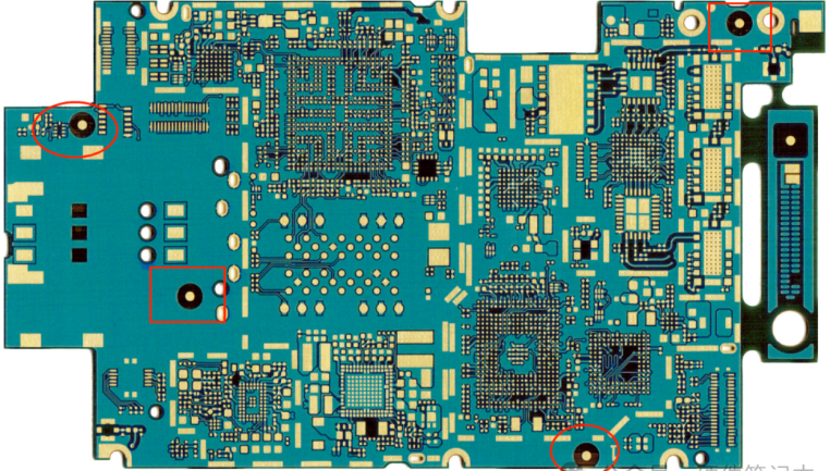
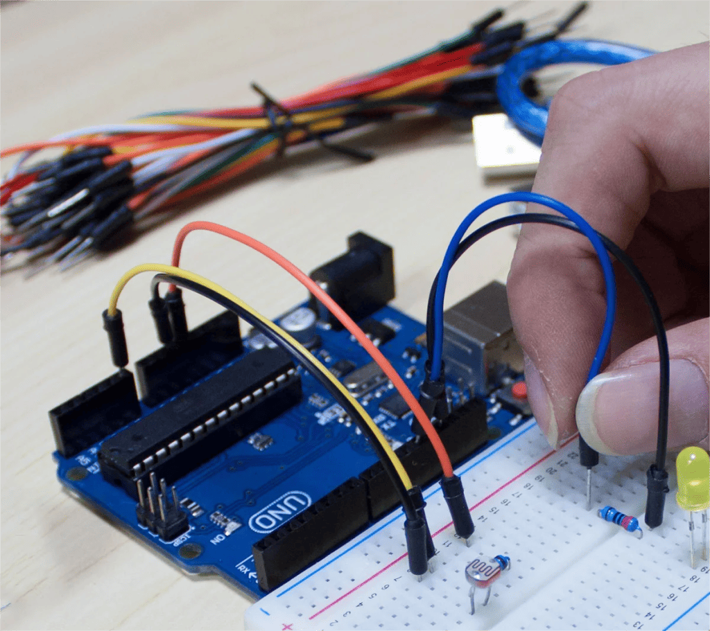
Double-sided PCBs feature conductive traces and pads on both the top and bottom copper layers, connected through plated vias, making them ideal for power supply design where routing density matters. Unlike single-sided boards, they support more complex circuits by allowing components on both sides, which improves PCB efficiency through shorter paths and better utilization of board real estate. In power supplies, this configuration handles input rectification, switching, and output filtering effectively while keeping costs lower than multilayer alternatives. Reliability improves as engineers can dedicate one side to high-current power paths and the other to control signals, reducing crosstalk. These boards excel in applications up to several hundred watts, where thermal management and current handling define success. Adhering to established guidelines ensures they meet performance needs without excessive complexity.
The relevance of double-sided PCB power supplies stems from their versatility in modern electronics, from consumer adapters to automotive modules. They provide sufficient layer count for ground planes and power distribution, critical for stable voltage regulation. Engineers value their manufacturability, as fabrication processes align with standard rigid board production. Why they matter becomes clear in scenarios demanding quick prototyping or volume production with tight budgets. Overall, they bridge the gap between simple single-layer designs and advanced high-density interconnects.
Core Technical Principles of PCB Layout in Power Supplies
Effective PCB layout in double-sided power supplies begins with strategic component placement to minimize parasitic inductance and resistance. High-power elements like inductors, capacitors, and switching transistors should cluster near the input and output edges, forming compact current loops. Control circuitry, including feedback loops and drivers, occupies the opposite side to isolate sensitive nodes from noisy power paths. Wide traces for high-current sections prevent voltage drops, following principles that balance electrical and thermal performance. Vias connect layers efficiently, but their placement avoids bottlenecks in heat flow or signal integrity.
Ground planes form the backbone of reliable layouts, poured generously on both sides where possible to shield signals and provide return paths. In double-sided designs, stitching vias tie the planes together, reducing impedance and EMI emissions. Power traces route directly with minimal bends to cut resistance, while signal lines stay perpendicular to avoid coupling. This structured approach enhances PCB efficiency by optimizing voltage delivery and minimizing losses. Engineers must consider board thickness and copper weight during schematic capture to align with fabrication capabilities.
Electromagnetic compatibility relies on loop area minimization, a key mechanism in switching power supplies. High di/dt paths from switch nodes pair closely with return paths, often using adjacent layers. Double-sided boards facilitate this by dedicating one layer to power and the other to ground, forming a pseudo-transmission line. Parasitic capacitance between layers aids filtering but requires spacing per voltage ratings. These principles ensure clean waveforms and compliance with noise limits.
Related Reading: Vias in Double-Sided PCBs: Connecting Layers Effectively
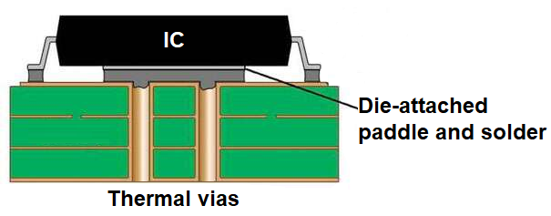
Thermal Management Strategies for Double-Sided PCB Power Supplies
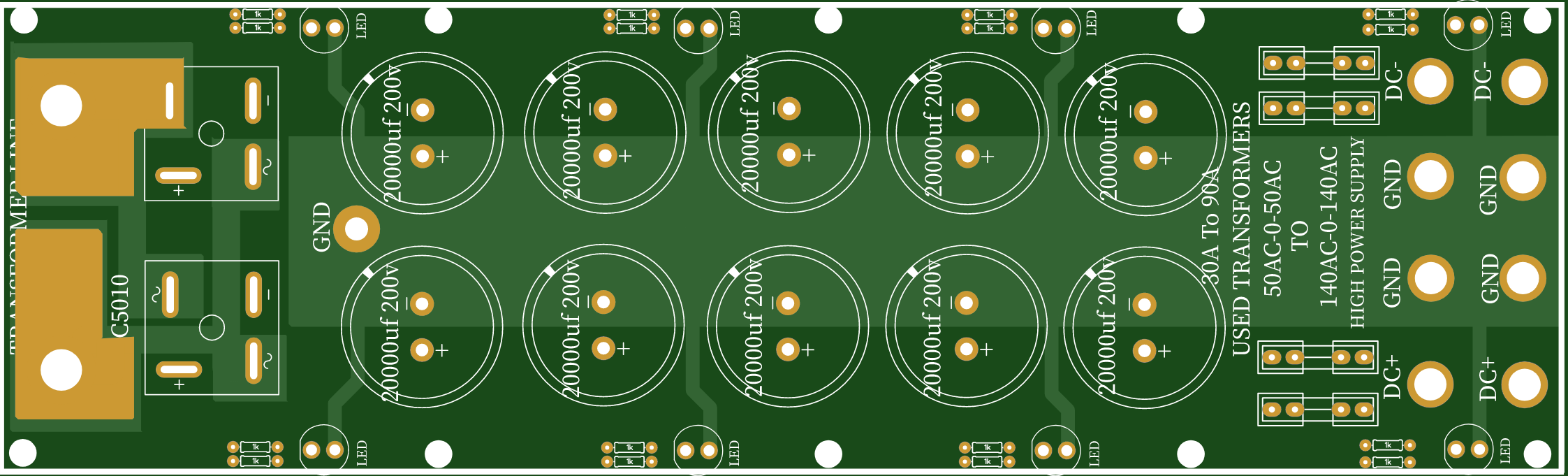
Thermal management stands as a cornerstone of reliable power supply design on double-sided PCBs, where heat from switching losses and conduction concentrates in specific areas. Copper pours act as heat spreaders, extending from hot components across unused board space to even out temperatures. Thermal vias, arrays of small plated holes under power devices, transfer heat to the opposite side or embedded heatsinks. Layer stacking influences this, with thicker copper foils enhancing conduction while standard dielectrics like FR-4 provide insulation. Engineers simulate hotspots early to refine via density and pour coverage.
In double-sided configurations, both sides contribute to dissipation, doubling effective surface area for convection or attachment to chassis. Heatsinks mount directly or via thermal pads, but clearance for airflow prevents recirculation. IPC-2221C guidelines inform thermal relief patterns on pads, ensuring solder joint integrity without impeding heat flow. Board edge cutouts or slots direct airflow over critical zones. These mechanisms sustain efficiency by keeping junction temperatures within safe margins.
Material choices impact thermal performance, with higher glass transition temperatures resisting warpage under load. Vias filled with conductive epoxy boost transfer rates in high-reliability builds. Monitoring involves infrared imaging during prototyping to validate models. Proper implementation prevents derating, extends component life, and upholds PCB efficiency.
Related Reading: Enhancing Heat Dissipation: Adding Heatsinks to Double-Sided PCBs
Best Practices for Optimizing Efficiency and Reliability
Start power supply design with schematic validation, ensuring decoupling capacitors shadow ICs closely. In PCB layout, assign the top side to primary power components for easy heatsinking, reserving the bottom for SMD passives and connectors. Route high-current paths first, using polygons for planes to fill voids and lower resistance. IPC-2152B charts guide trace widths based on current and allowable rise, preventing hotspots. Maintain 10-20% oversizing for margin in dynamic loads.
Signal integrity demands twisted pairs for differential feedback and guard traces around ADCs. EMI mitigation includes ferrite beads on inputs and snubbers across switches. For double-sided PCB power supplies, via fencing around noisy sections contains fields. Test points aid debugging without compromising integrity. These practices elevate PCB efficiency through low losses and stable regulation.
Fabrication alignment involves specifying controlled impedance for fast edges and annular ring sizes per IPC-6012F for via reliability. Solder mask dams prevent bridging on dense areas, while silkscreen labels input polarity clearly. Assembly sequences prioritize bottom-side reflow before top-side wave soldering. Post-process inspections verify continuity and isolation. Comprehensive DFM reviews catch issues early.
Common Challenges and Troubleshooting Insights
Engineers encounter overheating from inadequate via thermal coupling, resolved by increasing density or tenting unused pads. Voltage ripple spikes signal poor decoupling, fixed by closer cap placement and ground stitching. Warpage in reflow arises from asymmetric copper, balanced by mirror pours. EMI failures trace to long loops, shortened via rerouting. Systematic simulation and bench testing isolate causes logically.
Conclusion
Double-sided PCBs enable efficient, reliable power supply design through optimized layout, thermal strategies, and standards adherence. Key principles like plane pours, minimal loops, and thermal vias drive performance in constrained spaces. Best practices ensure manufacturability and longevity, making them a staple for electrical engineers. Prioritizing PCB efficiency yields stable outputs and reduced failures. Implementing these approaches positions designs for success across applications.
FAQs
Q1: What role does PCB layout play in double-sided PCB power supply efficiency?
A1: PCB layout directly impacts efficiency by minimizing trace resistance and inductance in power paths. Wide traces and copper pours reduce I-squared-R losses, while short loops cut switching inefficiencies. Proper separation of power and signal layers prevents noise coupling, stabilizing regulation. Thermal vias enhance heat spreading, preventing derating. Overall, thoughtful layout boosts conversion rates and sustains performance under load.
Q2: How does thermal management affect reliability in double-sided PCB power supplies?
A2: Thermal management ensures components operate below rated temperatures, averting failures from electromigration or dielectric breakdown. Vias and pours distribute heat evenly across both sides, leveraging natural convection. Heatsinks and airflow paths further aid dissipation in enclosed systems. Standards like IPC-2221C guide relief designs for joint reliability. Effective strategies extend MTBF and maintain PCB efficiency long-term.
Q3: Why choose double-sided PCBs for power supply design over single-sided?
A3: Double-sided PCBs offer dual-layer routing for complex power distribution and control, impossible on single-sided boards. They support ground planes on both sides for better EMI shielding and return paths. Component density rises, enabling compact designs with improved PCB efficiency. Cost remains low compared to multilayers, suiting moderate power needs. Reliability gains from balanced thermal profiles.
Q4: What are key considerations for trace routing in power supply PCB layout?
A4: Prioritize high-current traces with ample width per IPC-2152B to limit voltage drop and heating. Route switch nodes parallel to ground for low inductance. Avoid vias in power paths where possible to reduce resistance. Perpendicular signal routing minimizes crosstalk. Polygons fill spaces for uniform current sharing. These ensure reliable, efficient operation.
References
IPC-2221C — Generic Standard on Printed Board Design. IPC, 2023
IPC-2152B — Standard for Determining Current Carrying Capacity in Printed Board Trace. IPC, 2009
IPC-6012F — Qualification and Performance Specification for Rigid Printed Boards. IPC, 2023