ALLPCB


If you're working on a double-sided PCB design and wondering how to connect the layers efficiently, vias are the key. These small conductive pathways allow electrical signals and power to travel between the top and bottom layers of your board. In this blog, we'll dive deep into double-sided PCB vias, exploring via types, design rules, placement strategies, and best practices to ensure your PCB performs reliably. Whether you're a beginner or a seasoned engineer, you'll find actionable insights to improve your designs.
What Are Vias in Double-Sided PCBs?
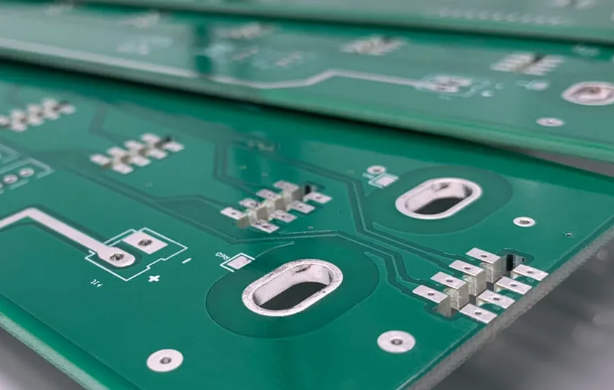
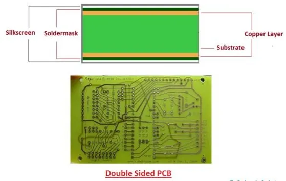
Vias are tiny holes drilled or formed in a printed circuit board (PCB) that create electrical connections between different layers. In a double-sided PCB, which has conductive copper layers on both the top and bottom, vias are essential for routing signals or power from one side to the other. Without vias, components on opposite sides of the board couldn’t communicate, limiting the complexity and functionality of your design.
In essence, vias act as bridges, ensuring seamless connectivity in compact designs where space is at a premium. Understanding how to use them effectively can make a significant difference in signal integrity, manufacturing costs, and overall board performance.
Why Vias Matter in Double-Sided PCB Design
Double-sided PCBs are a step up from single-sided boards, offering more space for components and traces by utilizing both sides of the board. However, this added flexibility comes with the challenge of connecting traces across layers. Vias solve this problem by providing a reliable pathway for electrical signals.
Effective via design and placement are critical for several reasons:
- Signal Integrity: Poorly placed vias can introduce noise or signal delays, especially in high-speed circuits where timing is crucial.
- Thermal Management: Vias can help dissipate heat by connecting to ground planes or thermal pads, preventing overheating.
- Space Efficiency: Vias allow for denser designs, reducing the need for larger boards and keeping costs down.
- Manufacturing Reliability: Properly designed vias reduce the risk of defects during production, such as incomplete plating or drilling errors.
By mastering via usage, you can create double-sided PCBs that are both functional and cost-effective.
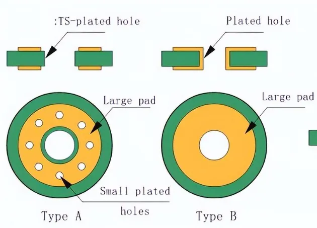
Types of Vias in Double-Sided PCBs
Not all vias are the same. Depending on your design needs, you can choose from several via types, each with specific applications in double-sided PCBs. Let’s break down the most common ones.
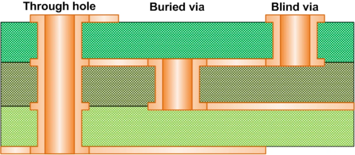
1. Through-Hole Vias
Through-hole vias are the most straightforward type, extending through the entire thickness of the PCB from the top layer to the bottom layer. They are typically plated with a conductive material, like copper, to ensure a strong electrical connection.
- Use Case: Ideal for simple double-sided designs where signals need to pass directly from one side to the other.
- Advantages: Easy to manufacture and cost-effective.
- Limitations: They take up space on both layers, which can limit routing options in dense designs.
2. Blind Vias
Blind vias connect an outer layer (top or bottom) to an inner layer but do not extend through the entire board. In double-sided PCBs, they are less common since there are no inner layers, but they can still be used in specific manufacturing processes.
- Use Case: Useful when transitioning to multilayer designs or when space on one side needs to remain free of vias.
- Advantages: Saves space on the opposite layer.
- Limitations: More expensive to produce due to precise drilling requirements.
3. Buried Vias
Buried vias connect internal layers without reaching the outer surfaces. In double-sided PCBs, they are rarely used since there are no internal layers, but they’re worth mentioning for engineers scaling up to multilayer designs.
- Use Case: Primarily for multilayer boards, not typical for double-sided PCBs.
- Advantages: Frees up surface space on both sides.
- Limitations: Complex and costly to manufacture.
4. Microvias
Microvias are smaller in diameter (typically less than 0.15 mm) and are often used in high-density designs. While more common in multilayer boards, they can be used in double-sided PCBs for advanced applications.
- Use Case: High-speed or compact double-sided designs requiring minimal space.
- Advantages: Allows for tighter routing and smaller board sizes.
- Limitations: Requires advanced manufacturing techniques, increasing costs.
Via Design Rules for Double-Sided PCBs
Designing vias for double-sided PCBs requires following specific rules to ensure functionality and manufacturability. These guidelines help minimize errors and optimize performance. Below are key via design rules to keep in mind.
1. Via Size and Drill Diameter
The size of a via, including its drill diameter and annular ring (the copper pad surrounding the via), must meet manufacturing capabilities. A typical drill diameter for through-hole vias in double-sided PCBs ranges from 0.2 mm to 0.8 mm, depending on the board’s complexity.
- Minimum Annular Ring: Ensure the copper ring around the via is at least 0.1 mm to 0.15 mm wide to prevent breakage during drilling.
- Aspect Ratio: Keep the via depth-to-diameter ratio below 10:1 for reliable plating. For a 1.6 mm thick board, avoid vias smaller than 0.16 mm in diameter.
2. Via Spacing
Vias placed too close together can cause manufacturing defects or signal interference. Maintain a minimum spacing of at least 0.2 mm between vias to avoid issues during drilling or plating.
3. Current Carrying Capacity
Vias must handle the current passing through them without overheating. A via with a 0.3 mm diameter can typically carry around 1-2 amps, depending on the copper thickness (e.g., 1 oz or 2 oz per square foot). Use multiple vias in parallel for higher currents to distribute the load.
4. Signal Integrity Considerations
In high-speed designs, vias can act as stubs or introduce impedance mismatches, causing signal reflections. For signals above 100 MHz, minimize via length and avoid unnecessary vias in critical signal paths. Aim for a controlled impedance, often around 50 ohms for many high-speed traces, by adjusting via size and placement.
Via Placement Strategies for Effective Layer Connection
Where you place vias on a double-sided PCB is just as important as their design. Poor placement can lead to routing issues, signal degradation, or manufacturing challenges. Here are some proven strategies for via placement.
1. Place Vias Near Components
Position vias close to the pins of components that need to connect to the opposite layer. This reduces trace length, minimizing signal delay and potential noise. For example, in a design with an IC requiring ground connection on the bottom layer, place a via directly adjacent to the ground pin.
2. Avoid Vias in High-Density Areas
In crowded sections of the board, vias can interfere with trace routing. Plan your layout to keep vias in less congested areas whenever possible, or use smaller microvias if space is tight.
3. Use Vias for Ground and Power Planes
For stable power delivery and noise reduction, use multiple vias to connect ground and power traces to their respective planes or layers. Distribute these vias evenly across the board to ensure uniform current flow and reduce voltage drops.
4. Minimize Via Stubs in High-Speed Designs
In high-speed circuits, unused portions of a via (stubs) can act as antennas, causing signal reflections. Place vias at the end of a trace or use back-drilling techniques to remove stubs if your design allows for it.
Common Challenges with Double-Sided PCB Vias
While vias are essential, they can introduce challenges if not handled properly. Here are some common issues and how to address them.
1. Signal Crosstalk
Placing vias too close to sensitive signal traces can cause crosstalk, especially in high-frequency designs. Maintain adequate spacing (at least 3x the via diameter) between vias and critical traces to minimize interference.
2. Manufacturing Defects
Improper via design, such as insufficient annular rings or overly small drill sizes, can lead to plating failures or broken connections. Always adhere to your manufacturer’s design guidelines, which often specify minimum tolerances like a 0.25 mm drill size for standard processes.
3. Thermal Stress
During soldering or operation, vias can experience thermal stress, leading to cracks or failures. Use thermal relief patterns (spokes connecting the via to a plane) to reduce stress and improve heat dissipation.
Best Practices for Double-Sided PCB Via Design
To wrap up, here are some best practices to ensure your double-sided PCB vias contribute to a high-performing design:
- Plan Early: Incorporate via placement into your initial layout planning to avoid routing conflicts later.
- Use Design Software: Leverage PCB design tools with built-in design rule checks (DRC) to catch errors in via size, spacing, or placement before manufacturing.
- Consult Manufacturer Guidelines: Different fabrication houses have varying capabilities. Confirm minimum via sizes and tolerances with your chosen provider.
- Test and Iterate: For critical designs, prototype your PCB to verify via performance, especially in high-speed or high-current applications.
Conclusion
Vias are the unsung heroes of double-sided PCBs, enabling effective layer connections that bring your designs to life. By understanding the different PCB via types, adhering to via design rules, and optimizing via placement, you can create reliable, high-performing boards tailored to your project’s needs. Whether you’re working on a simple hobby project or a complex industrial application, mastering double-sided PCB vias will elevate your design skills and ensure successful outcomes.
With these insights, you’re equipped to tackle via challenges head-on and build better PCBs. Keep experimenting with layouts, stay updated on manufacturing advancements, and always prioritize signal integrity and reliability in your designs.