 ALLPCB


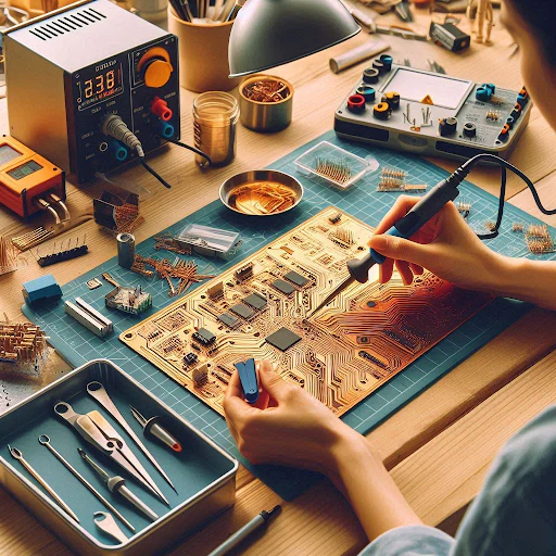
Introduction
Electronic hobbyists often face the challenge of turning innovative ideas into working prototypes without breaking the bank. Cheap PCB prototyping allows for rapid iteration, testing circuits on real hardware, and refining designs before scaling up. Methods like DIY PCB etching and the toner transfer method PCB offer hands-on control at minimal cost, while low-cost PCB fabrication services provide professional results for pennies per board. Discount PCB assembly options further reduce expenses by handling soldering tasks efficiently. These approaches empower makers to experiment freely, learn from failures, and achieve reliable outcomes. By focusing on budget-friendly techniques, hobbyists can maintain high quality without compromising functionality.
Why Budget-Friendly PCB Prototyping Matters for Electronic Hobbyists
Prototyping printed circuit boards on a budget accelerates the design-learn-test cycle essential for hobby projects. Hobbyists frequently iterate multiple versions to debug issues like signal integrity or power distribution, and high costs can stall progress. Affordable methods enable more trials, fostering deeper understanding of electronics principles. They also build skills in fabrication and assembly, valuable for future endeavors. In the end, cost savings translate to more projects completed and shared within communities. This matters because it democratizes access to custom hardware for personal inventions.
Core DIY Techniques for Cheap PCB Prototyping
The Toner Transfer Method PCB: A Staple for Hobbyists
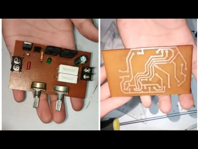
The toner transfer method PCB starts with printing a mirrored layout from design software onto glossy paper using a laser printer. Heat from a household iron transfers the toner onto a clean copper-clad board, creating a resist mask for etching. After etching, the paper lifts off easily with water, revealing the traces. This technique suits single-sided boards up to a few square inches, ideal for simple sensors or LED drivers. Cleanup involves removing excess toner with acetone for a polished finish. Hobbyists appreciate its repeatability with practice, often producing boards ready for components in under an hour.
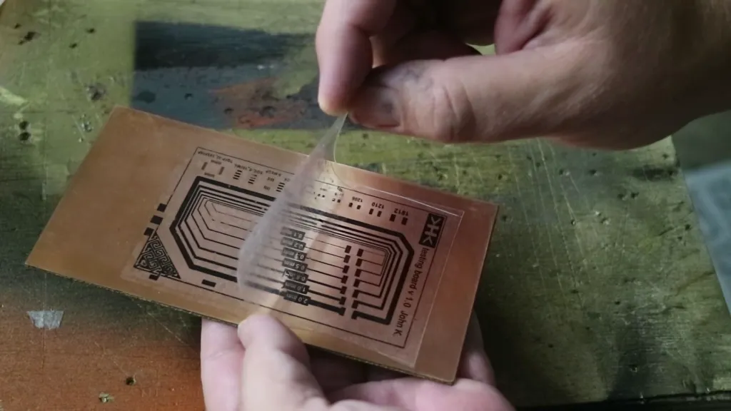
Common pitfalls include poor adhesion from insufficient heat or dirty boards, leading to under-etched traces. To mitigate this, preheat the copper and apply firm pressure evenly during transfer. Fine traces under 0.2mm demand high-resolution printing and glossy magazine pages for best results. Testing continuity with a multimeter post-etching ensures integrity before populating. This method shines for prototypes needing quick visual verification of routing.
DIY PCB Etching: Hands-On Chemical Fabrication
DIY PCB etching uses ferric chloride solution to dissolve unwanted copper after applying a resist pattern. Start by drawing or printing the layout on the board with a permanent marker or dry film photoresist for precision. Submerge the board in the etchant at room temperature, agitating gently for even removal, typically 10 to 30 minutes depending on concentration. Rinse thoroughly with water, neutralize residues, and strip the resist to expose the circuit. Safety gear like gloves and ventilation prevents skin burns or fumes. This process yields durable boards for moderate complexity projects.
Etchant regeneration with hydrogen peroxide and HCl extends usability, cutting recurring costs significantly. Monitor progress by inspecting edges; over-etching erodes traces while under-etching leaves shorts. For double-sided boards, align and tape the back to protect it during immersion. Post-etch inspection against IPC-A-600 acceptability criteria helps spot defects like pitting or incomplete etches early. Drying boards flat prevents warpage from residual moisture.
Leveraging Low-Cost PCB Fabrication Services
When DIY limits scale or complexity, low-cost PCB fabrication services deliver professional boards affordably. Order small quantities like five or ten pieces to keep per-unit prices under a dollar for basic two-layer designs. Optimize files by using standard panel sizes, 1oz copper, and FR-4 material to avoid surcharges. Specify solder mask and silkscreen only where essential, as these add minimal value for prototypes but inflate costs. Lead times of one to two weeks suit hobby timelines without rush fees. Compare quotes based on total cost including shipping for true savings.
Design choices heavily influence pricing; minimize vias, keep board size compact, and avoid odd shapes or tight tolerances. Services often bundle options like electrical testing at no extra charge for panels. Receiving boards with fiducials aids alignment for assembly. Even hobbyists benefit from these services for multilayer needs beyond DIY reach. Track orders meticulously to ensure specs match, preventing rework expenses.
Achieving Discount PCB Assembly Without Sacrificing Quality
Discount PCB assembly becomes viable through manual techniques or shared service runs. Hand-soldering with a fine-tip iron and flux suits through-hole components on prototypes, costing just time and basic supplies. For surface-mount, practice drag soldering or hot air rework stations available cheaply online. Group similar projects to amortize stencil costs if using services, dropping per-board assembly fees. Reference IPC J-STD-001 requirements for soldered joints to maintain reliability, focusing on fillet shapes and void minimization. This ensures hobby assemblies withstand vibration or heat cycles.
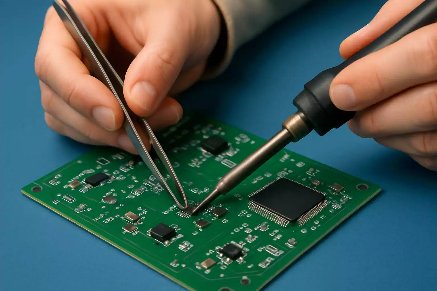
Pre-baking boards per JEDEC J-STD-020E prevents moisture-related defects during reflow, a free step saving failures. Use shared assembly panels to hit volume discounts, combining multiple hobby designs. Inspect joints visually against class 2 criteria for adequate coverage. Storage in dry boxes prolongs component life. These strategies yield functional prototypes rivaling commercial ones at fraction of cost.
Best Practices to Maximize Savings in PCB Prototyping
Streamline designs early by simulating circuits virtually to catch errors pre-fabrication. Choose component footprints from standard libraries to avoid custom work premiums. Panelize multiple boards per order, fitting as many as aspect ratios allow without waste. Select green solder mask as default, the cheapest color universally. Drill files with standard sizes reduce tooling charges. Adhering to IPC-6012E performance specs guides material choices for reliability.
Test prototypes incrementally: power rails first, then signals, using oscilloscopes or logic analyzers. Reuse stencils across batches by cleaning thoroughly. Bulk-buy consumables like etchant or solder paste for per-use savings. Document processes in notebooks for efficiency gains over projects. Collaborate in forums for shared tips on service hacks.
Troubleshooting Common Budget Prototyping Issues
Warpage from uneven etching or drying plagues DIY boards; bake at low heat post-process to flatten. Poor toner lift-off stems from glossy paper quality; experiment with magazine inks. Etch pits indicate contaminated copper; scrub with Scotch-Brite beforehand. Assembly bridges in SMT arise from excess paste; use syringes for precision. Continuity fails from undercuts; strengthen etchant and agitate. Systematic checks restore prototypes quickly.
Conclusion
Cheap PCB prototyping unlocks creativity for electronic hobbyists through DIY PCB etching, toner transfer method PCB, low-cost PCB fabrication services, and discount PCB assembly. These techniques balance affordability with functionality, enabling rapid development cycles. By applying best practices and referencing key standards, makers achieve professional-grade results on shoestring budgets. Experiment confidently, iterate often, and watch ideas become reality. Savings compound into more projects and skills gained.
FAQs
Q1: What is the toner transfer method PCB, and is it suitable for cheap PCB prototyping?
A1: The toner transfer method PCB involves printing mirrored layouts on glossy paper, ironing toner onto copper-clad boards, and etching away excess copper. It excels for single-sided prototypes under 100cm2, often costing under $1 per board excluding tools. Hobbyists value its speed and accessibility for testing simple circuits. Results match hobby needs when traces exceed 0.3mm, and practice improves yield for budget iterations.
Q2: How can hobbyists perform DIY PCB etching safely and affordably?
A2: DIY PCB etching uses ferric chloride to remove unprotected copper after applying resist via marker or toner. Work in ventilated areas with gloves to handle corrosive solutions safely. Regenerate etchant to reuse and keep costs low for dozens of boards. Agitate baths for uniform results in 15 to 30 minutes, then rinse and neutralize thoroughly. This method supports cheap PCB prototyping while teaching fabrication basics.
Q3: What tips help find low-cost PCB fabrication services for small runs?
A3: Optimize designs with standard thicknesses, panelization, and minimal layers to push prices below $5 for ten two-layer boards. Avoid exotics like thick copper or blind/buried vias. Bundle shipping for multiple orders and choose standard options like 1oz copper and FR-4. Specify basic finishes to prevent upcharges. These choices make low-cost PCB fabrication services accessible for hobby volumes while maintaining quality.
Q4: Are there discount PCB assembly options reliable for hobbyists?
A4: Manual assembly with a fine-tip iron and flux handles prototypes cheaply, and panel stencils enable service discounts for SMT. Follow IPC J-STD-001 for joint quality to avoid failures. Pre-bake moisture-sensitive parts and boards to sidestep reflow issues per JEDEC guidelines. Shared runs with community groups further reduce costs. When basics are observed, discount PCB assembly is dependable for functional testing.
References
IPC-A-600K — Acceptability of Printed Boards. IPC, 2020
IPC J-STD-001 — Requirements for Soldered Electrical and Electronic Assemblies. IPC, 2017
IPC-6012E — Qualification and Performance Specification for Rigid Printed Boards. IPC, 2017
JEDEC J-STD-020E — Moisture/Reflow Sensitivity Classification. JEDEC, 2014


