 ALLPCB


Embedded component PCB design integrates passive and active parts directly into the board layers rather than mounting them on the surface. This approach supports the compact size and performance demands of IoT devices that must operate reliably in constrained spaces while maintaining wireless connectivity and sensor functionality. Engineers adopt this method to reduce overall board area, shorten signal paths, and improve mechanical stability in applications such as environmental monitors and wearable sensors.
The technique aligns with broader trends in IoT PCB design where miniaturization directly influences product viability. By embedding components, designers achieve higher component density without increasing layer count excessively, which helps control manufacturing costs and board thickness. Low-power design becomes more achievable because shorter interconnects lower parasitic resistance and capacitance, reducing energy losses during operation.
Understanding Embedded Component PCB Design for IoT Applications
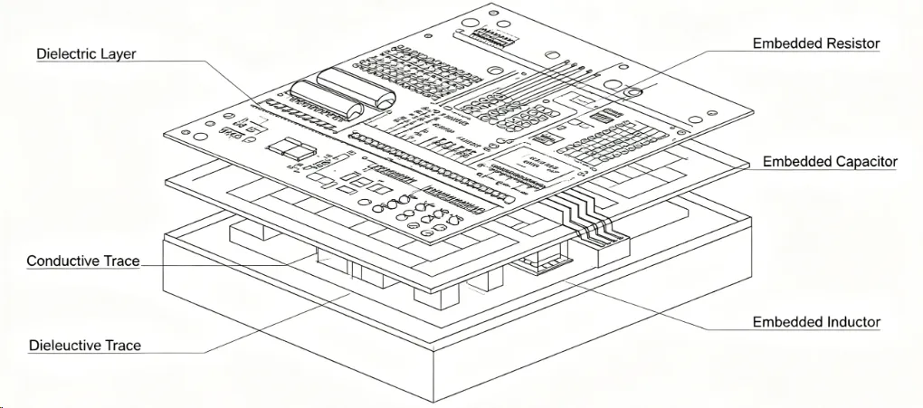
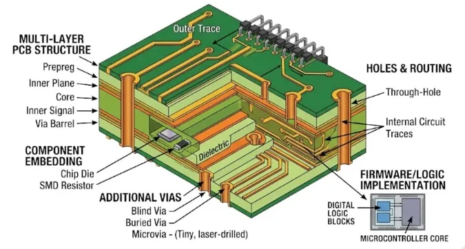
Embedded component technology places resistors, capacitors, and sometimes integrated circuits within the dielectric layers of a multilayer board. In IoT contexts this enables the integration of wireless communication modules and sensor interfaces in footprints that would otherwise exceed size limits. The result is a more robust assembly that withstands vibration and thermal cycling common in deployed devices.
Industry relevance stems from the need for reliable operation over extended periods on battery power. Embedded placement protects components from environmental exposure and mechanical stress, which supports consistent performance in remote or harsh locations. This design strategy also simplifies electromagnetic compatibility by allowing better ground plane continuity around sensitive RF sections.
Technical Principles of Embedded Component Integration
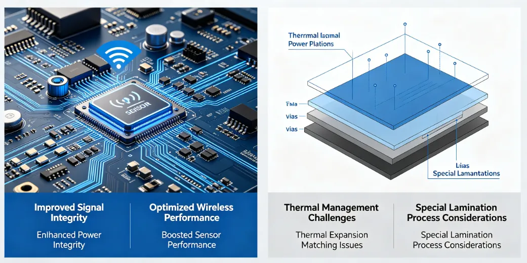
Signal integrity improves when components sit closer to active circuitry because trace lengths decrease and loop inductance drops. Power distribution networks benefit similarly, with embedded decoupling capacitors providing lower impedance paths to supply pins. Thermal management requires careful planning because embedded parts dissipate heat through surrounding copper and dielectric materials rather than direct airflow.
Low-power design principles emphasize minimizing quiescent current and optimizing sleep modes in microcontrollers paired with embedded sensors. Wireless communication sections demand precise impedance control around antennas and transmission lines, which embedded layouts can support through consistent dielectric properties. Sensor integration benefits from reduced noise pickup when analog front ends reside near the sensing elements inside the board stackup.
Designers must account for coefficient of thermal expansion mismatches between embedded components and the surrounding laminate to avoid stress during temperature excursions. Manufacturing processes involve sequential lamination where cavities or recesses accommodate the parts before final pressing. These steps influence yield and require adherence to established qualification procedures.
Related Reading: Embedded Components in PCB Design: Innovations and Use Cases
Practical Solutions and Best Practices
Begin layout by partitioning the board into functional zones that separate high-speed digital, analog sensor, and RF wireless areas. Place embedded passives near power pins of integrated circuits to enhance decoupling effectiveness while maintaining low-power operation. Route sensor signals with appropriate shielding and guard traces to preserve accuracy during integration.
For wireless communication, maintain consistent dielectric thickness around antenna feeds and avoid embedding conductive materials that could detune performance. Thermal vias or copper pours help conduct heat away from embedded active components when dissipation exceeds a few hundred milliwatts. Simulation of both electrical and thermal behavior before fabrication reduces iterations and supports reliable low-power targets.
Component selection should prioritize parts rated for the expected temperature range and moisture sensitivity level. Assembly sequences typically combine surface-mount technology with embedded placement, requiring process controls that prevent damage during lamination cycles. Following IPC-6012E guidelines for rigid board qualification helps ensure the final assembly meets performance specifications.
Sensor Integration and Wireless Considerations
Sensor integration in embedded designs places the transducer or its interface circuitry within the board to shorten analog paths and reduce susceptibility to interference. This arrangement supports accurate measurement of parameters such as temperature, humidity, or motion while keeping overall power consumption low. Calibration routines can account for any minor offsets introduced by the embedding process.
Wireless communication modules benefit from embedded placement of matching networks and filters that maintain signal integrity across operating bands. Antenna performance depends on ground plane integrity and clearance zones, which embedded layouts can preserve by strategic component positioning. Testing under representative conditions verifies that the combined sensor and radio functions meet system requirements without excessive current draw.
Related Reading: The Essential Guide to Embedded Component PCB Design Software
Conclusion
Embedded component PCB design offers a structured path to meet the size, power, and functionality needs of IoT devices. By focusing on signal integrity, thermal paths, and careful partitioning, engineers achieve reliable wireless communication and sensor performance in compact formats. Adherence to recognized qualification standards supports consistent manufacturing outcomes and long-term field reliability.
FAQs
Q1: What are the main advantages of embedded components in IoT PCB design?
A1: Embedded components reduce board size and improve electrical performance by shortening interconnects, which supports low-power design goals and reliable wireless communication in compact IoT devices. This approach also enhances mechanical robustness for deployed sensors.
Q2: How does embedded component placement affect low-power design in IoT applications?
A2: Shorter traces and optimized decoupling lower parasitic losses, enabling microcontrollers and sensors to operate with reduced energy consumption while maintaining wireless communication range and sensor integration accuracy.
Q3: What considerations apply to sensor integration on embedded PCBs for IoT?
A3: Designers position sensing elements and their interfaces to minimize noise and thermal effects, ensuring accurate data collection while preserving overall board compactness and low-power characteristics.
Q4: Which standards guide qualification of embedded component boards?
A4: IPC-6012E provides qualification and performance criteria for rigid printed boards that incorporate embedded elements, helping ensure the assembly meets electrical and mechanical requirements for IoT use.
References
IPC-6012E — Qualification and Performance Specification for Rigid Printed Boards. IPC, 2017
JEDEC J-STD-020E — Moisture/Reflow Sensitivity Classification. JEDEC, 2014
IPC-A-600K — Acceptability of Printed Boards. IPC, 2020





