 ALLPCB


In the fast-paced world of electronics, designing printed circuit boards (PCBs) with embedded components is becoming a game-changer. If you're searching for the right PCB design software to handle embedded component layouts, you're in the right place. This guide dives deep into embedded component PCB software, exploring essential tools, features, and best practices to help you create efficient, high-performance designs. Whether you're a seasoned engineer or just starting, you'll find actionable insights on selecting and using PCB design tools for embedded components.
What Are Embedded Components in PCB Design?
Embedded components in PCB design refer to electronic parts, such as resistors, capacitors, or even microchips, that are placed within the layers of a PCB rather than on its surface. This technique reduces the board's overall size, improves signal integrity, and enhances thermal management. For instance, embedding a 0.1 μF capacitor directly under a high-speed IC can reduce parasitic inductance and improve performance at frequencies above 100 MHz.
However, designing with embedded components requires specialized PCB design software. These tools must support advanced layer management, precise placement, and integration with manufacturing processes to ensure the components are correctly embedded without compromising the board's integrity.
Why Use PCB Design Software for Embedded Components?
Traditional PCB design tools focus on surface-mounted components, but embedded component designs demand more. Here's why dedicated PCB design software is critical:
- Space Efficiency: Embedding components can reduce board size by up to 30%, crucial for compact devices like wearables or IoT gadgets.
- Signal Integrity: Placing components closer to critical circuits minimizes trace lengths, reducing noise and improving signal speeds up to 5 Gbps in high-speed designs.
- Thermal Performance: Embedded components can dissipate heat more effectively within internal layers, lowering operating temperatures by 10-15°C in dense designs.
Without the right software, managing these benefits becomes a challenge. Embedded component PCB software offers specialized features like 3D visualization, layer-specific placement tools, and design rule checks (DRC) tailored for embedded layouts.
Key Features to Look for in Embedded Component PCB Software
Choosing the right PCB design tools for embedded components can make or break your project. Here are the must-have features to consider when selecting software:
1. Advanced Layer Management
Embedded components are placed within internal layers, so your software must allow precise control over layer stack-ups. Look for tools that support custom layer definitions and allow you to assign specific components to individual layers without errors. This is vital for maintaining a balanced stack-up with dielectric thicknesses as low as 0.1 mm for high-density designs.
2. 3D Visualization and Simulation
Seeing how embedded components fit within the board's structure is essential. 3D visualization helps identify potential issues like component overlap or insufficient clearance before manufacturing. Simulation tools can also predict signal integrity at frequencies up to 10 GHz, ensuring your design performs as expected.
3. Design Rule Checks (DRC) for Embedded Components
Standard DRCs may not account for the unique constraints of embedded components, such as via-in-pad requirements or minimum cavity sizes. Software tailored for embedded designs includes rules to check for proper embedding depth and alignment, preventing costly manufacturing errors.
4. Integration with Manufacturing Processes
Embedding components often requires specialized manufacturing techniques like laser drilling or sequential lamination. Your PCB design software should generate output files compatible with these processes, including precise Gerber files with embedded aperture data for cavities as small as 0.2 mm.
5. Library and Component Management
A robust library of pre-defined embedded components, including their 3D models and electrical parameters, saves time and reduces errors. Look for software that allows easy updates to component libraries and supports integration with supply chain databases for real-time availability.
Popular PCB Design Tools for Embedded Component Design
While many PCB design software options exist, only a few stand out for their ability to handle embedded components effectively. Below, we explore two leading platforms renowned for their capabilities in this area, focusing on their features for embedded layouts.
1. A Leading Industry Tool for Comprehensive Design
This widely-used software offers a powerful suite for PCB design, including robust support for embedded components. It provides advanced layer stack-up management, allowing designers to place components within specific layers with precision down to 0.01 mm. Its 3D visualization tools help engineers see the internal structure of the board, ensuring components are embedded without interference. Additionally, its simulation features can analyze signal integrity for traces operating at impedances as low as 50 ohms, ideal for high-speed applications.
2. A High-End Solution for Complex Layouts
Another top-tier option is a platform known for handling intricate PCB designs. It excels in embedded component placement with specialized DRCs that check for cavity dimensions and via placements. This software also integrates seamlessly with manufacturing workflows, supporting advanced techniques like HDI (High-Density Interconnect) with via diameters as small as 0.15 mm. Its thermal analysis tools can predict temperature rises in embedded designs, helping engineers optimize heat dissipation.
Benefits of Using Embedded Component PCB Software
Investing in the right PCB design tools for embedded components offers several advantages that directly impact the quality and efficiency of your projects. Here are some key benefits:
- Reduced Design Time: Automated features like pre-defined libraries and DRCs can cut design iterations by 20-30%, speeding up time-to-market.
- Improved Reliability: Precise placement and simulation reduce errors, leading to failure rates below 1% in production runs.
- Cost Savings: Smaller board sizes and fewer external components can lower material costs by up to 15% per design.
- Enhanced Performance: Embedding components near critical circuits can boost signal integrity, supporting data rates up to 10 Gbps in modern applications.
Challenges in Embedded Component PCB Design and How Software Helps
While the benefits are clear, designing with embedded components comes with unique challenges. Fortunately, modern PCB design software addresses many of these issues effectively.
1. Placement Precision
Embedding components requires exact placement to avoid misalignment during manufacturing. Software with high-precision grids (down to 0.001 mm resolution) ensures components are positioned accurately within cavities or layers.
2. Manufacturing Constraints
Not all manufacturers support embedded component technology due to the need for advanced processes like laser-drilled cavities. PCB design tools help by generating detailed fabrication notes and output files that specify requirements, such as cavity depths of 0.3 mm or dielectric constants of 4.2 for specific layers.
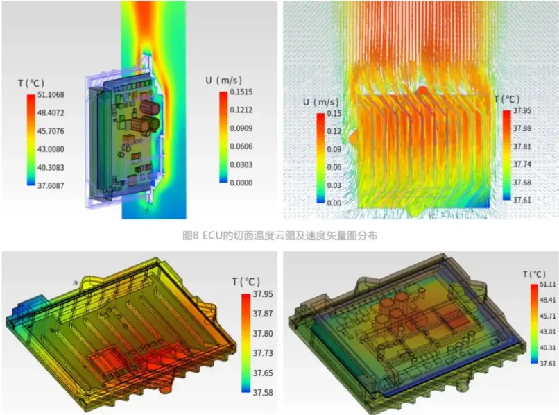
3. Thermal and Electrical Issues
Embedded components can create hotspots or interfere with signal paths if not designed properly. Advanced software offers thermal mapping to identify areas exceeding 85°C and signal analysis to ensure impedance matching within 5% tolerance.
Best Practices for Using PCB Design Software with Embedded Components
To get the most out of your embedded component PCB software, follow these best practices:
- Start with a Detailed Stack-Up Plan: Define your layer structure early, specifying which layers will house embedded components. Ensure dielectric thicknesses support embedding without compromising structural integrity.
- Use 3D Models for Validation: Always preview your design in 3D to check for clearance issues or component overlap before finalizing the layout.
- Leverage Simulation Tools: Run signal and thermal simulations to identify potential issues. For example, ensure high-speed signals maintain a 50-ohm impedance across embedded traces.
- Collaborate with Manufacturers: Share preliminary designs with your fabrication team to confirm that embedded component specifications, like cavity sizes of 0.5 mm, are feasible.
- Keep Libraries Updated: Regularly update component libraries to include the latest embedded parts, ensuring compatibility with current manufacturing standards.
How to Choose the Right Embedded Component PCB Software
Selecting the best PCB design software for your embedded component projects depends on several factors:
- Project Complexity: For high-density designs with multiple embedded layers, opt for software with advanced simulation and DRC features.
- Budget: Some tools offer tiered pricing, with basic versions suitable for smaller projects and premium editions for enterprise needs.
- Team Collaboration: If you work in a team, choose software with version control and cloud-based collaboration to streamline workflows.
- Learning Curve: Consider how user-friendly the software is, especially if your team includes beginners. Look for platforms with extensive tutorials and community support.
Future Trends in Embedded Component PCB Design Software
The field of embedded component design is evolving rapidly, and PCB design tools are keeping pace. Here are some trends to watch:
- AI-Driven Design: Artificial intelligence is being integrated into software to automate component placement and optimize signal paths, reducing design time by up to 40%.
- Cloud-Based Platforms: Cloud solutions enable real-time collaboration and access to powerful simulation tools without high-end hardware, supporting remote teams.
- Support for Advanced Materials: As PCBs use new substrates with dielectric constants below 3.0, software is adapting to simulate performance with these materials.
Conclusion: Elevate Your Designs with the Right PCB Software
Designing PCBs with embedded components offers incredible advantages, from shrinking board sizes to boosting performance. However, success hinges on using the right PCB design software tailored for embedded layouts. By focusing on features like layer management, 3D visualization, and manufacturing integration, you can tackle the challenges of embedded design and create reliable, high-quality boards.
At ALLPCB, we're committed to supporting your journey with resources and services that complement your design efforts. Whether you're refining a high-speed circuit or building a compact IoT device, choosing the right embedded component PCB software is the first step to achieving outstanding results. Dive into the tools and practices outlined in this guide, and take your PCB designs to the next level.


