ALLPCB


In the rapidly evolving world of edge computing, devices are increasingly deployed in challenging and harsh environments. From industrial plants to remote oil rigs, edge computing PCBs (Printed Circuit Boards) must withstand extreme temperatures, vibrations, shocks, and other stressors while maintaining reliable performance. This comprehensive guide explores how to design rugged edge computing PCBs tailored for harsh conditions, focusing on key aspects such as vibration resistance, thermal management, protective coatings, material selection, and shock testing. Whether you're an engineer or a designer, you'll find actionable insights to ensure your edge computing solutions thrive in the toughest settings.
Why Rugged Edge Computing PCBs Matter in Harsh Environments
Edge computing brings data processing closer to the source, reducing latency and improving efficiency in industries like manufacturing, energy, and transportation. However, the environments where these devices operate often expose PCBs to extreme conditions—think scorching deserts, freezing arctic zones, or high-vibration machinery. A poorly designed PCB can fail under such stress, leading to costly downtime or safety risks. Designing rugged PCBs for edge computing ensures durability, reliability, and long-term performance, no matter the challenge.
In this guide, we’ll dive deep into five critical areas: edge computing PCB vibration resistance, edge PCB thermal management, conformal coating for edge PCBs, PCB materials for extreme temperatures, and PCB shock testing for edge computing. Let’s get started with the foundational principles of rugged PCB design.
1. Edge Computing PCB Vibration Resistance: Building for Stability
Vibration is a common challenge in harsh environments, especially in industrial settings or vehicles where machinery and movement create constant stress on electronic components. Poor vibration resistance can lead to cracked solder joints, component detachment, or complete board failure. To ensure edge computing PCB vibration resistance, consider the following design strategies:
- Component Placement and Mounting: Position heavier components closer to mounting points or areas with structural support to minimize movement. Use secure mounting hardware like screws or brackets to anchor the PCB firmly to the enclosure.
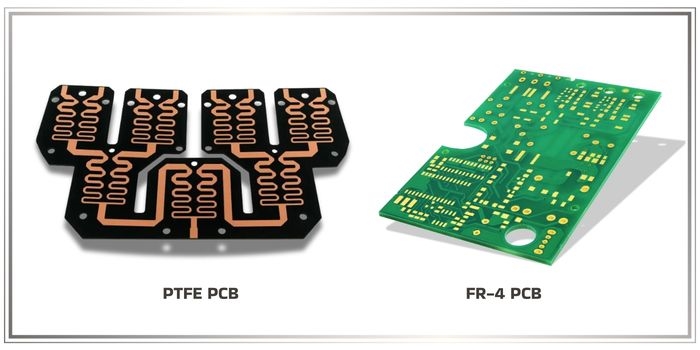
- Board Thickness and Material: Opt for thicker PCBs (e.g., 2.0 mm or more) to increase rigidity. Materials like FR-4 with high glass transition temperatures (Tg) can also help withstand mechanical stress.
- Reinforcement Techniques: Add stiffeners or ribs to the PCB design to reduce flexing. For extreme cases, consider underfilling or staking components to lock them in place.
- Vibration Testing: Simulate real-world conditions using vibration testing equipment. Test at frequencies ranging from 10 Hz to 2000 Hz, which covers most industrial vibration profiles, to identify weak points in the design.
By focusing on these elements, you can significantly enhance the durability of your edge computing PCBs against vibrations, ensuring uninterrupted operation in dynamic environments.
2. Edge PCB Thermal Management: Keeping Cool Under Pressure
Thermal management is critical for edge computing PCBs, especially in environments with extreme temperatures or limited airflow. Overheating can degrade components, reduce lifespan, and cause system failures. Effective edge PCB thermal management requires a multi-faceted approach:
- Heat Sink Integration: Attach heat sinks to high-power components like processors or power regulators to dissipate heat. Ensure proper thermal interface materials (TIMs) with conductivity values of at least 1-2 W/m·K for efficient heat transfer.
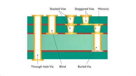
- Thermal Vias: Incorporate thermal vias under heat-generating components to transfer heat to other layers or a heat sink. A grid of vias with a diameter of 0.3 mm and spacing of 1.2 mm can improve heat dissipation by up to 30%.
- Layer Stackup Design: Use multilayer boards with dedicated ground planes to spread heat evenly across the PCB. Copper thickness of 2 oz or higher on power planes can also aid in heat distribution.
- Component Selection: Choose components with wide operating temperature ranges (e.g., -40°C to 85°C or broader for industrial-grade parts) to ensure reliability in fluctuating conditions.
Proper thermal management not only prevents failures but also extends the operational life of edge computing devices in harsh climates or enclosed systems with minimal ventilation.
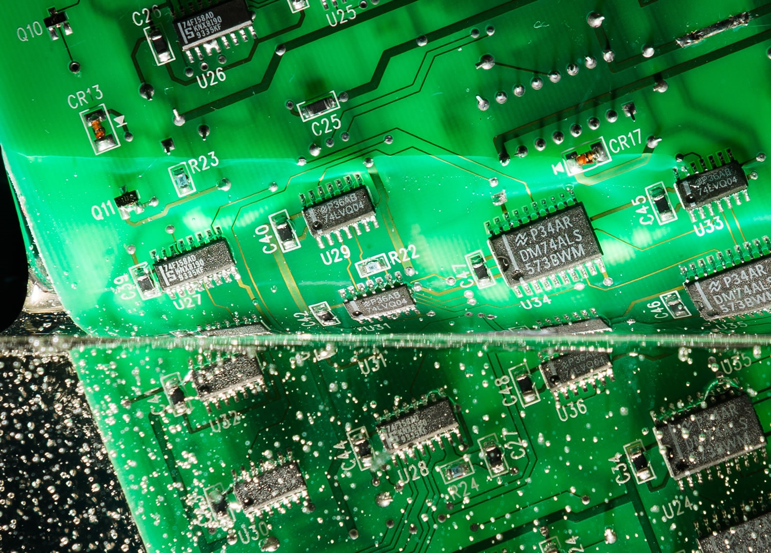
3. Conformal Coating for Edge PCBs: Shielding Against Environmental Threats
Harsh environments often expose PCBs to moisture, dust, chemicals, and salt spray, which can lead to corrosion or short circuits. Conformal coating for edge PCBs provides a protective barrier that safeguards the board and its components. Here’s how to approach this critical protection method:
- Types of Coatings: Common conformal coatings include acrylic, silicone, polyurethane, and epoxy. Silicone coatings, for instance, offer excellent flexibility and temperature resistance (up to 200°C), making them ideal for extreme conditions.
- Application Methods: Apply coatings via brushing, spraying, or dipping, ensuring uniform coverage of 25-75 microns in thickness. Avoid coating connectors or test points by using masking techniques.
- Environmental Resistance: Select a coating based on specific threats. For high-humidity areas, polyurethane coatings provide superior moisture resistance, while silicone excels in thermal shock scenarios.
- Testing and Inspection: After application, inspect the coating under UV light (if it’s UV-curable) to ensure complete coverage. Test for adhesion and flexibility to confirm the coating won’t crack under stress.
Conformal coatings act as a first line of defense, protecting edge computing PCBs from environmental damage and ensuring long-term reliability in hostile settings.
4. PCB Materials for Extreme Temperatures: Choosing the Right Foundation
The choice of materials is fundamental when designing edge computing PCBs for extreme temperatures. Standard materials may warp, crack, or lose electrical properties under thermal stress. Here’s what to consider when selecting PCB materials for extreme temperatures:
- High-Tg FR-4: For moderate temperature ranges (-40°C to 130°C), high-Tg FR-4 (Tg of 170°C or higher) offers a cost-effective solution with good mechanical and electrical properties.
- Polyimide: For higher temperature extremes (up to 260°C), polyimide laminates provide excellent thermal stability and low thermal expansion, ideal for aerospace or oil and gas applications.
- Ceramic-Based Materials: In ultra-high temperature scenarios, ceramic substrates like alumina or aluminum nitride can operate beyond 300°C while offering superior heat dissipation.
- Coefficient of Thermal Expansion (CTE): Match the CTE of the PCB material to that of components (typically 3-6 ppm/°C for ceramics) to prevent cracking during thermal cycling.
Selecting the right material ensures that your edge computing PCB can endure temperature swings without compromising structural integrity or performance.
5. PCB Shock Testing for Edge Computing: Ensuring Durability Under Impact
In harsh environments, edge computing devices may face sudden impacts or drops, especially in military, automotive, or industrial applications. PCB shock testing for edge computing helps validate a design’s ability to withstand such events. Here’s how to approach shock testing and design for impact resistance:
- Shock Testing Standards: Follow standards like MIL-STD-810G, which specifies shock tests with peak acceleration of 50g for 11 milliseconds to simulate real-world impacts.
- Design Considerations: Reinforce solder joints with stronger alloys (e.g., SAC305) and use smaller, lighter components to reduce stress during impact. Avoid tall components that could act as levers under shock.
- Enclosure Protection: House the PCB in a rugged enclosure with shock-absorbing materials like rubber gaskets or foam padding to dampen impact forces.
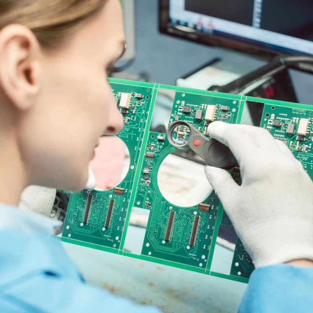
- Post-Test Analysis: After testing, inspect for microcracks, delamination, or component displacement using X-ray imaging or visual microscopy to identify failure points.
Shock testing and thoughtful design ensure that edge computing PCBs can survive unexpected impacts, maintaining functionality in even the most demanding conditions.
Additional Tips for Rugged Edge Computing PCB Design
Beyond the core areas discussed, here are a few additional considerations to enhance the ruggedness of your edge computing PCBs:
- IP Ratings for Enclosures: Aim for enclosures with IP65 or higher ratings to protect against dust and water ingress, common in harsh environments.
- Redundancy in Design: Build redundancy into critical circuits to ensure failover capability if a component fails under stress.
- Simulation Tools: Use simulation software to model thermal, vibration, and shock scenarios before prototyping. This can save time and reduce costly iterations.
These extra steps can make a significant difference in the overall reliability of your edge computing solutions.
Conclusion: Building Resilient Edge Computing PCBs for Any Challenge
Designing rugged edge computing PCBs for harsh environments requires careful attention to multiple factors, from vibration resistance and thermal management to material selection and protective coatings. By prioritizing edge computing PCB vibration resistance, implementing effective edge PCB thermal management, applying conformal coating for edge PCBs, choosing suitable PCB materials for extreme temperatures, and conducting thorough PCB shock testing for edge computing, you can create boards that perform reliably no matter the conditions.
At ALLPCB, we understand the unique challenges of designing for harsh environments and are committed to supporting engineers with high-quality manufacturing and expert guidance. Whether you’re working on industrial IoT, remote monitoring, or other edge computing applications, use these strategies to build durable, high-performance PCBs that stand the test of time.