ALLPCB


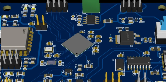
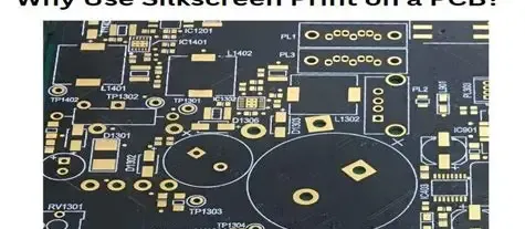
Black silkscreen, also known as legend or marking ink, provides essential component identifiers, polarity marks, and assembly instructions on printed circuit boards. When selected in black rather than the more common white, it introduces specific design for manufacturability factors that affect visibility, adhesion, and compatibility with downstream processes. Engineers must evaluate these choices early to avoid yield losses during fabrication and assembly. Proper planning ensures the silkscreen meets both functional and visual requirements without compromising board integrity.
Why Black Silkscreen Matters for Manufacturability
Black silkscreen offers high contrast against certain solder mask colors and copper finishes, improving readability during manual inspection and automated optical inspection. In high-density designs, this contrast reduces the risk of misinterpretation of reference designators and pin-one indicators. However, the darker pigment can interact differently with curing processes and surface finishes compared to lighter inks. Manufacturers apply silkscreen after solder mask but before final surface finish in many flows, making early design decisions critical for process compatibility. Considering these elements during layout helps maintain consistent quality across production volumes.
Technical Principles of Black Silkscreen Application
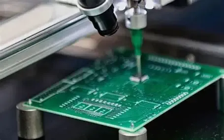
Silkscreen ink consists of epoxy or acrylic resins mixed with pigments and fillers that determine opacity and adhesion. Black formulations typically use carbon-based pigments that provide excellent light absorption but require precise control of ink thickness to avoid excessive buildup. Application methods include screen printing for high-volume runs and direct legend printing for finer features. Curing occurs through thermal or UV exposure, and incomplete curing can lead to poor adhesion or outgassing during reflow. Industry standards such as IPC-A-600 define acceptability criteria for legend legibility and placement accuracy, guiding both designers and fabricators.
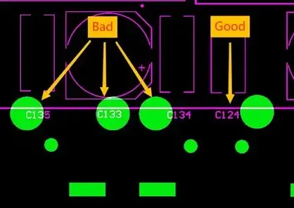
The interaction between black silkscreen and solder mask involves chemical compatibility and thermal expansion matching. Mismatched coefficients can cause cracking or delamination during temperature cycling. In addition, black ink may absorb more heat during reflow soldering, potentially affecting local board temperature profiles. Designers account for these factors by specifying minimum clearance from pads and traces, typically following guidelines that prevent ink migration onto contact areas. These principles ensure the silkscreen remains intact throughout the product lifecycle.
Key DFM Considerations for Black Silkscreen
Placement rules require adequate spacing from component pads, vias, and board edges to prevent ink from interfering with soldering or electrical performance. Minimum character height and line width must align with the chosen printing method to achieve reliable resolution. Black silkscreen can exhibit lower visibility under certain lighting conditions compared to white, so designers often increase font sizes or add supplementary markings. Warpage induced by uneven ink distribution represents another concern, particularly on thin substrates.
Surface finish compatibility also influences outcomes. Finishes such as ENIG or immersion silver may alter ink adhesion characteristics, requiring adjusted curing parameters. Thickness control remains essential because excessive ink can create topography issues during stencil printing of solder paste. Thermal profiling during assembly must accommodate any additional heat absorption from the black pigment. Addressing these variables early in the design phase reduces the likelihood of rework or scrap.
Best Practices for Silkscreen Design and Application
Engineers should generate silkscreen layers with consistent orientation and font styles to support automated reading systems. Limiting the total ink coverage area minimizes potential warpage and simplifies curing. Specifying ink type and color explicitly in fabrication notes helps manufacturers select appropriate materials and processes. Review of the silkscreen layer during design for manufacturability checks catches issues such as overlapping text or insufficient clearances before production begins.
Collaboration between design and manufacturing teams ensures that legend placement supports both assembly and field service needs. Using vector-based artwork rather than raster images preserves edge definition during scaling. Verification against IPC-6012 qualification requirements confirms that the finished board meets performance expectations for legend durability. These practices collectively improve first-pass yield and reduce time to market.
Potential Challenges and Mitigation Strategies
One common challenge involves reduced contrast in low-light environments or when viewed through conformal coating. Mitigation includes strategic placement of critical markings away from shadowed areas and selection of matte-finish inks. Another issue arises from ink bleeding during application, which can be addressed through optimized screen mesh and viscosity control. Thermal stress during multiple reflow cycles may degrade adhesion, so accelerated life testing helps validate material choices.
Designers also monitor for interactions with other processes such as laser marking or barcode application. When black silkscreen covers large areas, it can affect the board's overall emissivity and influence thermal management. Early simulation of these effects, combined with prototype builds, provides data for final adjustments. Consistent documentation of all silkscreen parameters supports traceability and continuous improvement.
Conclusion
Black silkscreen introduces distinct manufacturability considerations that extend beyond simple color selection. Attention to contrast, adhesion, placement clearances, and process compatibility enables reliable production while maintaining readability. By integrating these factors into the design workflow and referencing established standards such as IPC-A-600 and IPC-6012, engineering teams achieve higher yields and more robust assemblies. Early collaboration with fabrication partners further strengthens outcomes across the product lifecycle.
FAQs
Q1: How does black silkscreen affect PCB manufacturability compared to white?
A1: Black silkscreen provides different contrast levels and heat absorption characteristics that influence curing, adhesion, and reflow behavior. Designers must adjust clearances and verify compatibility with surface finishes to maintain process stability. These adjustments help prevent defects while preserving legend functionality throughout assembly.
Q2: What are the main silkscreen design rules for DFM?
A2: Key rules include minimum character size, line width, and spacing from pads and traces to ensure reliable printing and prevent interference with soldering. Proper layer orientation and coverage limits also reduce warpage risks. Following these guidelines improves yield and supports automated inspection.
Q3: Why is black silkscreen chosen for certain PCB applications?
A3: Black silkscreen offers superior contrast against light-colored solder masks or metallic finishes, aiding visual inspection and reducing errors during assembly. It also supports aesthetic requirements in consumer or industrial products. Selection depends on lighting conditions, inspection methods, and thermal profile considerations.
Q4: How can engineers verify silkscreen quality during PCB manufacturing?
A4: Verification involves checking legend legibility, adhesion, and placement accuracy against acceptance criteria defined in relevant industry standards. Visual inspection combined with adhesion testing on sample boards confirms performance. Documentation of ink type and curing parameters supports consistent results across batches.
References
IPC-A-600K — Acceptability of Printed Boards. IPC, 2020
IPC-6012E — Qualification and Performance Specification for Rigid Printed Boards. IPC, 2017