ALLPCB


Crosstalk represents a significant signal integrity challenge in printed circuit board design, particularly as operating frequencies increase and board densities rise. It occurs when electromagnetic energy from one signal trace couples into an adjacent trace, potentially distorting data and degrading overall system performance. Engineers working on high-speed digital and mixed-signal boards must address this phenomenon early in the layout process to maintain reliable operation. Understanding its mechanisms allows for targeted design choices that reduce unwanted interactions without excessive cost or complexity. Effective management of PCB crosstalk supports compliance with performance expectations in demanding applications.
What Is PCB Crosstalk and Why It Matters
PCB crosstalk is the unwanted transfer of signals between adjacent conductors on a board. It manifests primarily as near-end crosstalk, measured at the transmitting end of the victim trace, and far-end crosstalk, observed at the receiving end. Both types arise from capacitive and inductive coupling that intensifies with higher frequencies, longer parallel trace lengths, and reduced spacing. In modern electronics, where data rates exceed several gigabits per second, even modest crosstalk levels can cause bit errors, timing violations, or electromagnetic interference issues. Addressing crosstalk early helps preserve signal quality and reduces the need for later corrective measures during testing or production.
Industry standards such as IPC-2221 provide guidance on trace spacing and layout practices that help control coupling effects in printed board designs.
Technical Principles and Mechanisms
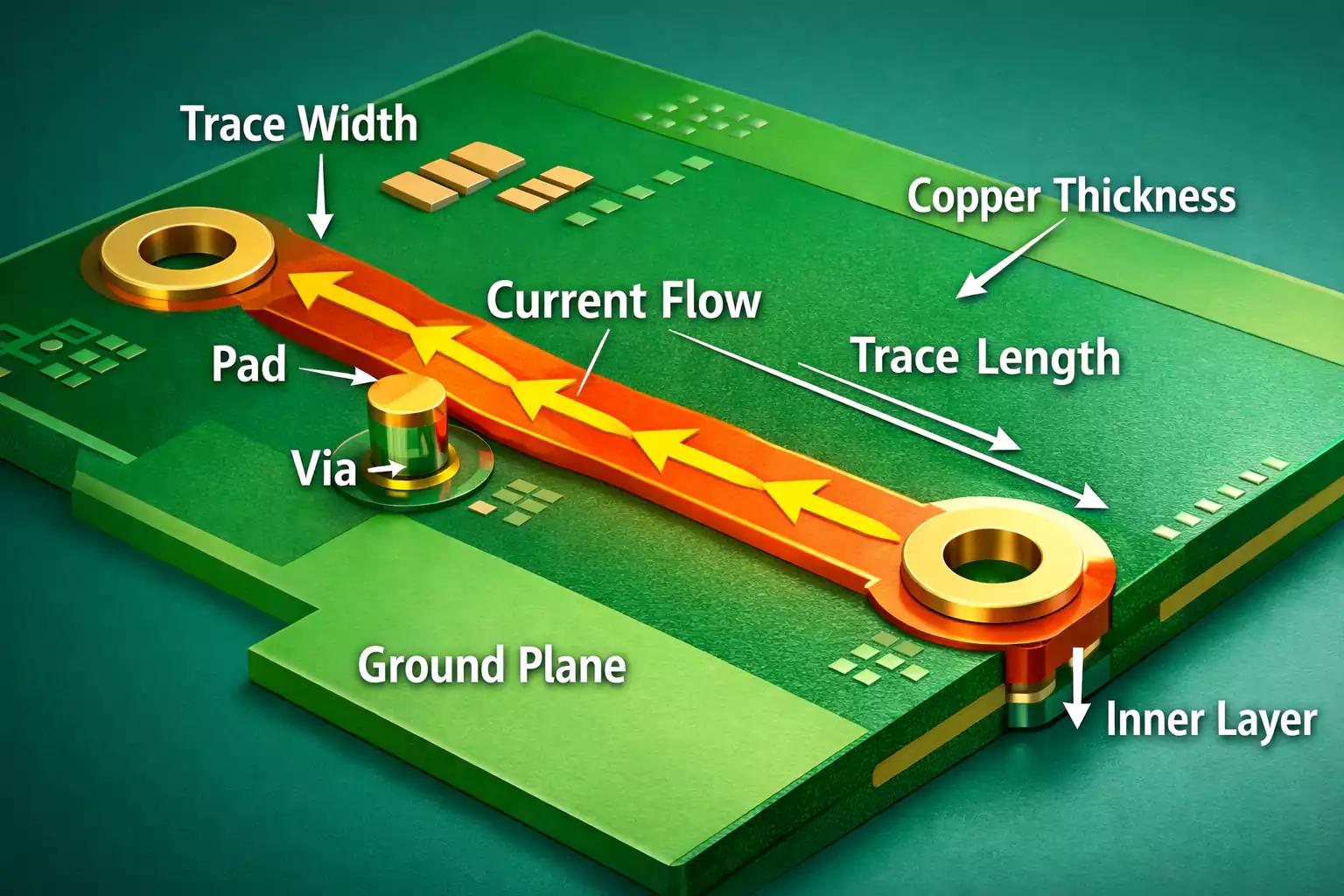
Crosstalk develops through two primary coupling paths. Capacitive coupling transfers energy via the electric field between traces, proportional to the mutual capacitance and the rate of voltage change on the aggressor line. Inductive coupling occurs through the magnetic field, driven by mutual inductance and current variations. The relative strength of each mechanism depends on the dielectric constant of the board material, trace geometry, and return path configuration. Parallel routing over significant lengths amplifies both effects, while discontinuities such as vias or layer changes can further complicate the coupling profile.
Near-end crosstalk typically produces a positive pulse that reflects back toward the driver, whereas far-end crosstalk can appear as a negative pulse at the receiver. Factors including trace width, height above the reference plane, and dielectric thickness directly influence coupling coefficients. Higher frequencies exacerbate the issue because the wavelength shortens relative to trace dimensions, increasing the efficiency of energy transfer. Structured analysis of these parameters during schematic and layout phases enables prediction of potential problem areas before fabrication.
Identification Methods
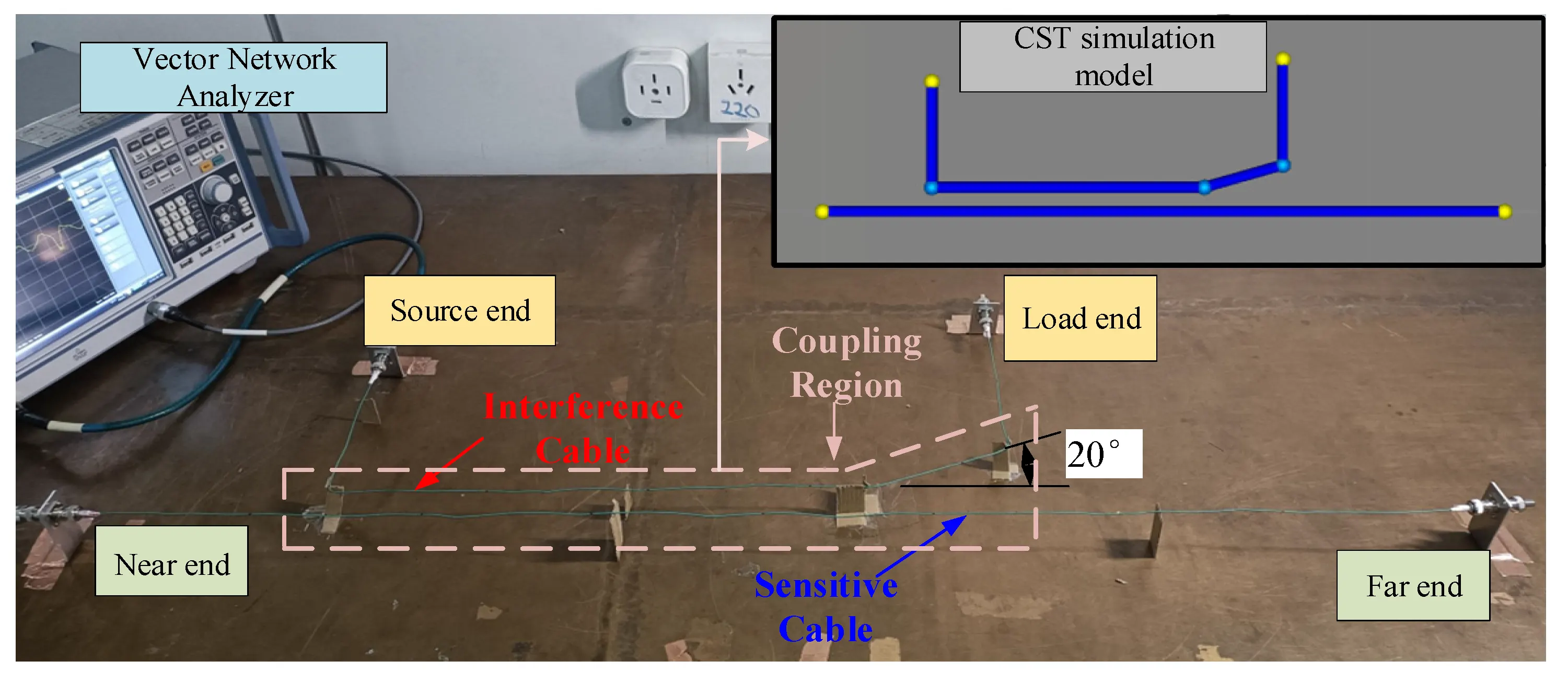
Engineers identify PCB crosstalk through a combination of simulation and measurement. Time-domain reflectometry and vector network analyzer measurements reveal coupling magnitudes at specific frequencies. Eye diagram analysis on prototype boards shows the cumulative impact on signal quality, including jitter and amplitude reduction attributable to crosstalk. Simulation tools model the board stack-up and routing to estimate near-end and far-end crosstalk values before physical prototypes exist. Systematic review of parallel trace segments and their lengths relative to signal rise times provides an initial screening for high-risk areas.
Practical Solutions and Best Practices for Crosstalk Mitigation and Prevention
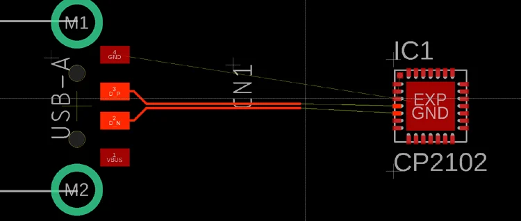
Several layout techniques reduce PCB crosstalk effectively. Increasing the physical separation between critical traces lowers both capacitive and inductive coupling coefficients. Routing signals on adjacent layers with orthogonal orientations minimizes parallel overlap. Placing a solid ground or power plane between signal layers provides shielding and establishes a consistent return path. Differential pair routing with controlled spacing and tight coupling within the pair rejects common-mode noise while reducing susceptibility to external coupling.
Termination strategies, such as proper resistive matching at line ends, absorb reflections that could otherwise interact with coupled energy. Guard traces or ground pours placed between sensitive lines offer additional isolation when spacing alone proves insufficient. Minimizing via stubs and controlling impedance throughout the signal path further limits discontinuities that amplify crosstalk. Following established design rules for trace geometry and layer stack-up ensures consistent results across production boards.
IPC-2221 outlines recommended practices for trace spacing and reference plane usage that support effective crosstalk control in printed board designs.
Additional prevention measures include careful assignment of high-speed signals to inner layers where possible and avoiding long parallel runs of unrelated signals. When layer changes are necessary, providing adequate ground vias near signal vias maintains return path continuity. Regular design reviews that incorporate crosstalk estimates help catch issues before they reach manufacturing. These practices collectively contribute to robust signal integrity without requiring exotic materials or excessive board area.
Conclusion
Effective management of PCB crosstalk requires attention to coupling mechanisms, proactive identification during design, and disciplined application of spacing, shielding, and termination techniques. By integrating these approaches with guidance from standards such as IPC-2221, engineers achieve reliable high-speed performance while maintaining manufacturability. Consistent application across projects reduces debugging time and improves overall product quality.
FAQs
Q1: What causes PCB crosstalk in high-speed designs?
A1: PCB crosstalk arises primarily from capacitive and inductive coupling between adjacent traces when signals switch at high frequencies. Parallel routing, insufficient spacing, and inadequate return paths increase coupling strength. Proper stack-up design and trace separation according to established guidelines help limit its occurrence.
Q2: How can near-end crosstalk be distinguished from far-end crosstalk?
A2: Near-end crosstalk appears at the driver end of the victim trace as a reflected pulse, while far-end crosstalk reaches the receiver end. Measurement setups using time-domain instruments or frequency-domain analysis allow engineers to quantify each type separately and apply targeted mitigation.
Q3: What layout practices support crosstalk mitigation and prevention?
A3: Increasing trace separation, using ground planes for shielding, routing differential pairs, and avoiding long parallel runs represent core practices. Termination at line ends and controlled impedance throughout the path further reduce the impact of coupled energy on signal integrity.
Q4: Why does PCB crosstalk matter for electric engineers working on dense boards?
A4: In dense, high-frequency designs, PCB crosstalk can degrade timing margins and introduce errors that affect system reliability. Early identification combined with proven prevention techniques ensures designs meet performance targets without costly iterations.