 ALLPCB


Introduction
In PCB assembly, ensuring defect-free production is critical for reliability, especially in high-density designs with surface-mount components. Electric engineers often face the choice between automated optical inspection (AOI) and X-ray inspection when troubleshooting assembly issues. Comparing X-Ray and AOI helps identify the best fit based on defect types, production volume, and board complexity. AOI excels at surface-level checks, while X-ray reveals hidden problems under components. This article explores their principles, strengths, and practical applications to guide selection for optimal quality control. Understanding X-Ray vs AOI cost and defect detection capabilities allows teams to balance thoroughness with efficiency.
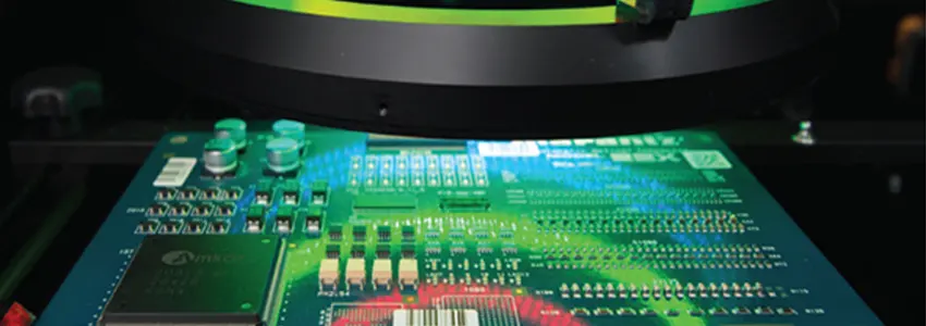
What is Automated Optical Inspection (AOI)?
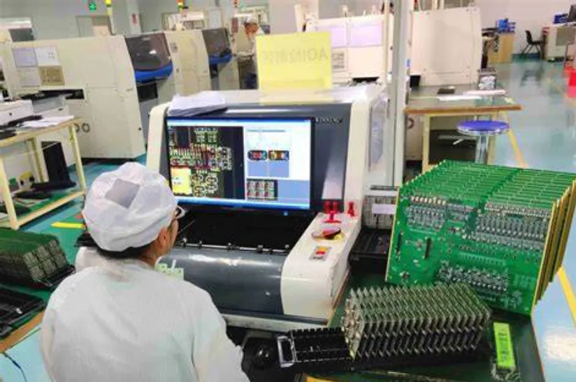
AOI uses high-resolution cameras and multiple light sources to capture images of the PCB surface during assembly. Systems project structured light patterns or employ ring and coaxial illumination to highlight features like solder joints and component placement. Software compares these images against a golden board reference or CAD data to flag deviations. This method suits post-print, pre-reflow, and post-reflow stages for quick verification. Engineers rely on AOI for its repeatability in detecting visible anomalies without physical contact. Troubleshooting common issues like bridging becomes straightforward with real-time feedback.
What is X-Ray Inspection?
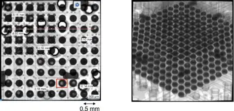
X-ray inspection, often automated as AXI, generates radiographic images by passing X-rays through the PCB to differentiate densities of materials like solder, copper, and silicon. Detectors capture transmitted rays, producing grayscale images where voids appear as dark spots and dense areas as brighter regions. This non-destructive technique penetrates components such as BGAs and QFNs to assess hidden solder joints. Operators adjust voltage and current for optimal contrast on multilayer boards. In practice, it aids failure analysis by quantifying issues like void percentages. Electric engineers use it when surface methods fall short for internal integrity.
Technical Principles Behind AOI and X-Ray
AOI operates on optical principles, relying on reflected visible light to resolve features down to microns on exposed surfaces. Multiple angles and wavelengths enhance shadow-free imaging for accurate fillet shape assessment. In contrast, X-ray follows Beer-Lambert attenuation laws, where ray intensity decreases exponentially through matter based on thickness and atomic number. This enables 2D or 3D tomographic views for volumetric analysis. Both methods employ AI-driven algorithms for classification, but AOI processes simpler pixel data while X-ray handles complex density maps. Selecting between them depends on whether defects are superficial or subsurface.
X-Ray vs AOI Defect Detection Capabilities
When comparing X-Ray and AOI defect detection, AOI shines for open-view issues like missing parts, polarity errors, tombstoning, and excessive solder. It reliably spots misalignment or lifted leads by measuring offsets against tolerances. X-ray, however, uncovers invisible faults such as head-in-pillow, insufficient ball height in BGAs, or microcracks in vias. AOI misses under-component voids that compromise thermal and electrical performance, while X-ray quantifies solder volume for joint reliability. In troubleshooting, AOI serves as a first-pass filter, escalating suspects to X-ray for confirmation. This layered approach maximizes yield without over-inspection.
- Surface Defects: AOI strengths include component presence, bridges, fillets; X-ray is limited for surface-only checks.
- Hidden Defects: AOI is limited; X-ray strengths include voids, cracks, BGA offsets.
- Resolution: AOI is high for visible features; X-ray provides density-based internal detail.
X-Ray vs AOI Cost Considerations
X-Ray vs AOI cost differs significantly due to equipment complexity and operational demands. AOI systems feature affordable optics and cameras, with lower maintenance from non-radiative components. X-ray requires robust generators, shielded enclosures, and certified technicians, driving up capital and running expenses. Inline AOI fits high-volume lines economically, while X-ray often operates offline or as sampling stations. Engineers weigh these against risk: simple boards favor AOI savings, but critical assemblies justify X-ray investment. Long-term, combining both optimizes total cost of ownership through reduced escapes.
Strengths and Limitations of X-Ray and AOI
X-Ray AOI strengths lie in their complementary roles: AOI delivers speed for 100% coverage, catching 80-90% of common faults early. Its limitations include shadowing by tall components or reflective surfaces that obscure joints. X-ray strengths cover those gaps with penetration power, ideal for double-sided or cavity-down packages. Yet, it struggles with throughput on large panels and demands skilled interpretation of artifacts like beam hardening. Neither is foolproof alone; false calls from AOI need manual review, while X-ray's grayscale ambiguity benefits from oblique angles. Practical setups integrate both per IPC-A-610 guidelines for solder joint acceptability.
When to Use X-Ray vs AOI in PCB Assembly
Use AOI for standard SMT lines with exposed joints, such as QFP or SOIC packages, to maintain pace without bottlenecks. Reserve X-ray for high-reliability boards featuring BGAs, LGAs, or fine-pitch arrays where hidden defects pose failure risks. In prototyping, AOI verifies placement post-print, while X-ray confirms reflow integrity per J-STD-001 soldering requirements. High-mix, low-volume runs benefit from flexible X-ray sampling, avoiding AOI reprogramming overhead. Troubleshoot escapes by cross-referencing: AOI flags for visual, X-ray for root cause. Hybrid strategies ensure compliance without excess cost.
Best Practices for Implementing AOI and X-Ray
Calibrate AOI lighting and thresholds regularly to match board variations, reducing false positives from gloss or dirt. Program golden samples with diverse tolerances for robust detection across lots. For X-ray, select kV/mA settings per layer count and use 3D if available for tilt analysis. Train operators on artifact recognition and integrate with SPI for paste validation. Document inspections linking to traceability for audits. Follow sequential flow: SPI, AOI pre/post-reflow, X-ray on critical zones to align with quality standards.
Real-World Troubleshooting Insights
Consider a BGA assembly failing functional tests: AOI passes surface but X-ray reveals 15% voiding from flux residue. Adjust profile per J-STD-001, re-reflow, and re-inspect. For bridging epidemics, AOI pinpoints stencil wear, while X-ray checks via fill. In multilayer HDI, X-ray detects barrel cracks missed by optics. These cases underscore when to use X-Ray AOI together for yield ramps. Engineers log trends to refine processes proactively.
Conclusion
Choosing between X-ray and AOI hinges on balancing speed, cost, and coverage for your PCB assembly needs. AOI handles routine surface checks efficiently, while X-ray tackles hidden threats in complex designs. Comparing X-Ray and AOI reveals no single winner; instead, their strengths enhance overall quality. Implement based on component tech and risk profile for reliable outcomes. This targeted approach minimizes escapes and supports scalable production.
FAQs
Q1: What are the main differences in X-Ray vs AOI defect detection?
A1: AOI detects surface issues like component misalignment and solder bridges using optical imaging, ideal for quick line scans. X-ray penetrates to reveal internal voids and BGA offsets invisible to optics. Use AOI for visible faults and X-ray for subsurface in high-density assemblies. This comparison ensures comprehensive coverage without redundancy.
Q2: How does X-Ray vs AOI cost impact selection?
A2: AOI offers lower upfront and operational costs with simple optics, suiting high-volume runs. X-ray demands pricier generators and shielding, justified for critical BGAs. Factor throughput: AOI for inline, X-ray sampling. Engineers prioritize based on defect risk versus budget for optimal ROI.
Q3: What are X-Ray AOI strengths in PCB quality control?
A3: AOI strengths include fast 100% inspection of placement and fillets; X-ray excels at quantifying hidden solder volume. Together, they cover surface to internal per standards. Troubleshoot by escalating AOI flags to X-ray for confirmation. This duo boosts yield in SMT lines.
Q4: When to use X-Ray AOI in assembly processes?
A4: Deploy AOI pre/post-reflow for standards compliance; add X-ray for BGAs or failures. High-rel apps demand both for voids and bridges. Sample X-ray on complex boards to control costs. Practical integration prevents escapes effectively.
References
IPC-A-610 — Acceptability of Electronic Assemblies. IPC
J-STD-001 — Requirements for Soldered Electrical and Electronic Assemblies. IPC


