ALLPCB


Introduction
Reverse engineering a printed circuit board assembly (PCBA) involves a meticulous process of disassembly and analysis to uncover its design, functionality, and potential weaknesses. Electric engineers often undertake PCBA reverse engineering analysis to troubleshoot failures, support legacy systems, or evaluate third-party hardware. This approach reveals hidden defects that impact long-term performance and exposes security risks in supply chains. By combining non-destructive and destructive techniques, engineers can assess material integrity, solder joint quality, and component authenticity. Ultimately, such analysis ensures that PCBA reliability in reverse engineering aligns with operational demands in critical applications. The following sections detail the methodologies and best practices for effective evaluation.
The relevance extends to compliance with industry benchmarks, where reverse engineering verifies adherence to assembly standards. Without it, engineers risk deploying unreliable boards that fail under thermal or mechanical stress. Security implications grow as interconnected devices multiply, making PCBA security testing essential for IoT and embedded systems. Reliability data from reverse engineering informs predictive maintenance models and redesign efforts. Thus, it bridges the gap between manufacturing and field performance.

What Is PCBA Reverse Engineering and Why It Matters
PCBA reverse engineering analysis starts with recreating the schematic, bill of materials, and layout from a physical assembly without original documentation. Engineers document every layer, trace, via, and component to map electrical connections and firmware interactions. This process matters because modern electronics face increasing threats from counterfeit parts and design flaws that compromise system integrity. In industries like aerospace and medical devices, identifying these issues prevents catastrophic failures and extends product lifecycles. Moreover, PCBA vulnerability assessment through reverse engineering detects intentional backdoors or hardware trojans that evade software scans. For electric engineers, mastering this skill optimizes procurement and enhances overall system resilience.
The relevance extends to compliance with industry benchmarks, where reverse engineering verifies adherence to assembly standards. Without it, engineers risk deploying unreliable boards that fail under thermal or mechanical stress. Security implications grow as interconnected devices multiply, making PCBA security testing essential for IoT and embedded systems. Reliability data from reverse engineering informs predictive maintenance models and redesign efforts. Thus, it bridges the gap between manufacturing and field performance.
Technical Principles of PCBA Reverse Engineering
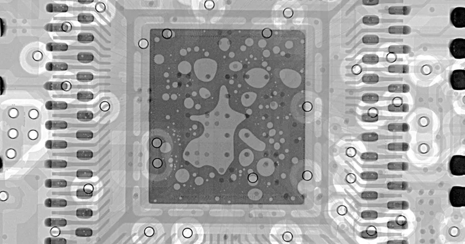
The foundation of PCBA reverse engineering lies in layered inspection techniques that progress from surface-level to internal structures. Initial visual examination identifies component markings, solder anomalies, and board warpage using magnification tools. Electrical continuity testing maps nets without powering the board, revealing opens or shorts in traces. X-ray imaging penetrates BGA packages and multi-layer stacks to visualize hidden solder balls and voids. These non-destructive methods preserve the assembly for further probing if needed. Engineers correlate findings with expected performance to flag deviations early.
Destructive techniques become necessary for deeper insights, such as controlled delayering with chemical etching or mechanical milling. This exposes inner copper layers, dielectrics, and via plating for metallographic analysis. Cross-sectioning a sample slice under a microscope assesses laminate adhesion and barrel fill in vias. Component decapsulation reveals die markings and bond wires, crucial for authenticity checks. Each step follows precise protocols to avoid introducing artifacts that skew results. PCBA reverse engineering analysis thus builds a comprehensive failure mode database.
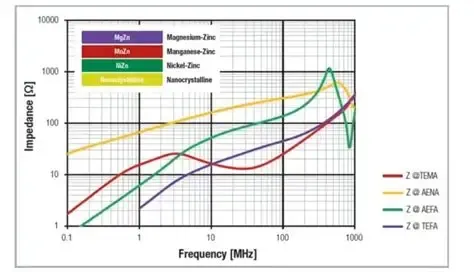
Thermal and mechanical stress simulations recreate operational conditions post-analysis. Vibration tables and thermal chambers test extracted components for endurance limits. Signal integrity analysis using TDR equipment identifies impedance mismatches in high-speed traces. These principles ensure that reliability assessments reflect real-world usage. Vulnerabilities like thin trace routing or inadequate ground planes emerge clearly through this structured approach.
Assessing PCBA Reliability in Reverse Engineering
PCBA reliability in reverse engineering hinges on evaluating solder joints, materials, and assembly processes against established criteria. Microscopic inspection checks for head-in-pillow defects, tombstoning, or bridging per IPC-A-610J guidelines. Dye-and-pry tests quantify adhesive strength between components and boards, predicting delamination risks. Bake and preconditioning cycles simulate aging to detect popcorn cracks in moisture-sensitive parts. Statistical sampling from multiple boards establishes process capability indices for consistent quality. Engineers prioritize high-risk areas like power planes and connectors during this phase.
Material analysis involves FTIR spectroscopy for resin composition and SEM for contamination detection. Trace width measurements verify current-carrying capacity under IPC-6012F specifications. Thermal cycling exposes CTE mismatches between dissimilar materials, leading to fatigue cracks. Accelerated life testing extrapolates mean time between failures using Arrhenius models. Documentation of these metrics supports root cause analysis for field returns. Reliability assessment thus transforms empirical data into actionable design improvements.
Mechanical integrity checks include shear and pull testing on soldered leads. Warpage measurements with shadow moire interferometry quantify bow and twist limits. These evaluations reveal vulnerabilities from poor lamination or via drilling. Integrating reliability data from reverse engineering refines future prototypes. Electric engineers benefit from this holistic view to mitigate risks proactively.
PCBA Vulnerability Assessment and PCBA Security Testing
PCBA vulnerability assessment focuses on hardware-level threats beyond firmware exploits. Physical inspection hunts for unauthorized jumpers, debug ports, or epoxy blobs hiding chips. Supply chain analysis cross-references component datasheets against markings for counterfeits. Side-channel analysis measures power consumption or EM emissions during operation to infer keys or states. Fault injection via laser or glitch generators tests resilience to tampering attempts. These methods uncover subtle weaknesses like shared power domains enabling crosstalk attacks.
PCBA security testing incorporates protocol decoding on buses like I2C or SPI to detect unencrypted data flows. Firmware dumping from flash chips reveals hardcoded credentials or backdoors. Die photography post-decap compares against known good samples for trojan circuits. Environmental exposure tests assess physical attack vectors, such as acid etching traces. Compliance with standards like IPC-7711/7721 during deassembly ensures accurate vulnerability mapping without collateral damage. Engineers document attack surfaces in a risk matrix for mitigation strategies.
Advanced techniques like chip-off forensics recover data from non-responsive NAND storage. Netlist comparison against reference designs flags malicious modifications. Electromagnetic probing localizes cryptographic operations for further analysis. These practices elevate PCBA security testing to prevent zero-day exploits. Integrating vulnerability findings with reliability data strengthens overall board hardening.
Best Practices for PCBA Reverse Engineering Analysis
Adopt a phased approach starting with non-destructive tests to maximize data yield. Calibrate all equipment per manufacturer specs and maintain ESD-safe environments. Document every step with high-resolution photography and 3D scans for traceability. Use standardized rework procedures from IPC-7711/7721 to remove components without damage. Collaborate with cross-functional teams for specialized analyses like failure mode effects. Validate extracted schematics through simulation before physical prototyping.
Prioritize safety by handling chemicals in fume hoods and disposing of etchants properly. Employ statistical tools to analyze defect populations across samples. Update analysis protocols based on emerging threats like quantum-resistant crypto needs. Train personnel on latest inspection criteria to ensure consistency. These practices enhance PCBA vulnerability assessment accuracy and efficiency.
Troubleshooting Common Challenges in Reverse Engineering
Engineers frequently encounter multilayer boards where blind vias complicate net tracing. Employ layer-by-layer peeling with plasma etching for precise isolation. Multi-chip modules resist standard decap, requiring focused ion beam milling instead. Correlate X-ray densities with material databases to differentiate stacked dice. Solder mask removal demands controlled abrasion to avoid substrate damage. Addressing these hurdles systematically improves PCBA reliability in reverse engineering outcomes.
Obscured markings from conformal coatings require solvent stripping followed by UV fluorescence. High-density interconnects benefit from serial probing with flying leads. Firmware obfuscation challenges demand JTAG boundary scans for memory dumps. Practical troubleshooting refines techniques over iterations. Electric engineers leverage these insights for robust analyses.
Conclusion
PCBA reverse engineering analysis provides electric engineers with unparalleled insights into reliability and security. By systematically evaluating solder integrity, material durability, and potential attack vectors, professionals mitigate risks effectively. Adhering to standards like IPC-A-610J and IPC-7711/7721 ensures reproducible results. Integrating non-destructive and destructive methods yields comprehensive data for design enhancements. Ultimately, this discipline safeguards critical electronics against failures and threats. Engineers equipped with these skills drive innovation and dependability in complex systems.
FAQs
Q1: What role does IPC-A-610J play in PCBA reverse engineering analysis?
A1: IPC-A-610J establishes acceptability criteria for solder joints, component placement, and cleanliness during PCBA reverse engineering analysis. Engineers use it to benchmark defects like voids or misalignments observed under microscopy. This standard guides quantitative assessments, ensuring reliability evaluations align with industry norms. Consistent application prevents overlooking subtle issues that affect long-term performance.
Q2: How does PCBA vulnerability assessment identify hardware trojans?
A2: PCBA vulnerability assessment involves decapping suspicious chips and imaging bond wires for anomalous circuitry. Netlist extraction compares against functional models to detect hidden logic. Side-channel monitoring flags irregular power draws indicative of trojans. These steps, combined with supply chain verification, expose threats early. Electric engineers prioritize high-value components for thorough checks.
Q3: Why is PCBA security testing crucial in reverse engineering?
A3: PCBA security testing during reverse engineering uncovers physical attack points like exposed test pads or weak glues. Protocol sniffing reveals insecure communications, while fault injection simulates real exploits. This testing complements reliability checks by addressing intentional weaknesses. Engineers document findings to inform shielding and encryption upgrades. Proactive measures enhance system trustworthiness.
Q4: How to ensure PCBA reliability in reverse engineering processes?
A4: PCBA reliability in reverse engineering requires thermal cycling extracted components and shear testing joints per standards. Cross-sectioning verifies via integrity and plating thickness. Statistical analysis of multiple samples predicts field performance. Documentation supports iterative improvements. This methodical approach minimizes deployment risks for engineers.