 ALLPCB


Introduction
In modern electronics, high-speed designs demand robust signal integrity to handle increasing data rates and complex routing needs. An 8-layer PCB stackup provides the necessary layers for separating signals, power, and ground while minimizing interference. This configuration supports optimizing 8-layer PCB performance by enabling better impedance matching and reduced noise. Engineers face challenges like crosstalk and reflections, but a well-planned stackup addresses these effectively. As designs evolve toward faster interfaces, mastering 8-layer PCB stackup design becomes essential for reliable operation. This guide explores key strategies drawn from established engineering principles.
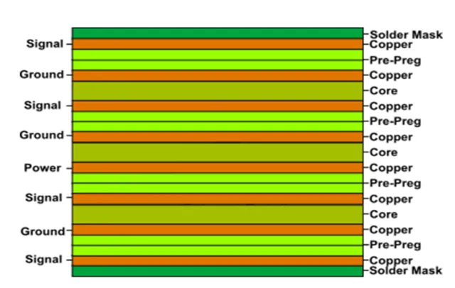
What Is an 8-Layer PCB Stackup and Why It Matters
An 8-layer PCB stackup refers to the precise arrangement of eight alternating copper foil and dielectric layers, defining the board's electrical and mechanical properties. Each layer serves a specific role, such as carrying signals, distributing power, or providing ground references. This multilayer structure allows for denser component placement and more routing options compared to simpler boards. Signal integrity improves because inner layers can be shielded, reducing external noise coupling. For electric engineers, understanding stackup directly impacts high-frequency performance and compliance with design guidelines like those in IPC-2221B. Ultimately, it matters because poor stackup leads to failures in data transmission, while optimized designs ensure stability in demanding applications.
The relevance grows with rising clock speeds, where even minor discontinuities cause errors. Multiple planes enable dedicated sections for analog and digital signals, preventing noise bleed. Power delivery becomes more uniform across the board, supporting high-current components. Thermal management also benefits from balanced layer distribution. In summary, an effective 8-layer stackup unlocks higher performance without excessive cost increases.
Core Technical Principles of 8-Layer PCB Stackups
Signal propagation in multilayer boards relies on controlled electromagnetic fields between traces and reference planes. High-speed signals require low-loss paths with consistent characteristic impedance to avoid reflections. Dielectric materials between layers influence propagation delay and attenuation. Return currents flow through adjacent ground planes, forming tight loops that minimize inductance. Discontinuities like vias or plane splits disrupt this balance, amplifying issues. Proper layer sequencing ensures each signal layer neighbors a reference plane for stable fields.
Crosstalk arises from capacitive and inductive coupling between adjacent traces. Near-end crosstalk affects launch points, while far-end impacts receivers. Ground planes shield layers, confining fields and reducing coupling. Impedance mismatches occur from varying geometries or material inconsistencies. Simulations reveal these effects early, guiding adjustments. Adhering to principles like plane adjacency maintains integrity across frequencies.
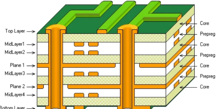
Mastering 8-Layer PCB Stackup Impedance Control
8-layer PCB stackup impedance control starts with defining trace geometries relative to reference planes. Outer layers often operate as microstrips with air exposure, while inner layers form striplines fully embedded in dielectric. Consistent spacing to planes ensures predictable impedance for single-ended and differential pairs. Variations in dielectric constant affect velocity and matching, so uniform materials aid control. Engineers calculate based on stackup parameters to target values suitable for the signals. Tolerance windows depend on fabrication capabilities, emphasizing collaboration with manufacturers.
Power-aware stackups integrate impedance alongside plane capacitance for filtering. Splitting planes requires careful via fencing to avoid gaps. Pre-layout models predict behavior, allowing tweaks before routing. Post-fabrication coupons verify actual values against specs. This process integrates seamlessly with overall design flow. Effective control preserves waveform shape over long traces.
Strategic 8-Layer PCB Ground Plane Placement
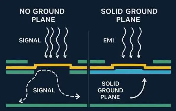
The 8-layer PCB ground plane strategy focuses on providing low-impedance return paths for every signal layer. Positioning ground planes immediately adjacent to high-speed signal layers creates shielding and confines fields. Multiple ground planes distribute return currents evenly, reducing bounce. Solid planes without large splits maintain continuity, as cuts create high-inductance paths. Stitching vias around splits or edges reinforce integrity. In mixed-signal boards, separate analog and digital grounds connect at a single point to avoid loops.
Power planes pair with grounds for decoupling, but separation prevents direct coupling to signals. Symmetric placement around the board center minimizes warpage during lamination. Ground pours on signal layers fill unused areas, aiding balance. This strategy enhances EMI suppression by acting as shields. Overall, it forms the backbone of reliable performance. Per IPC-6012D, plane quality directly ties to board qualification.
Effective 8-Layer PCB Crosstalk Reduction Techniques
8-layer PCB crosstalk reduction leverages plane shielding and routing discipline. Sandwiching signal layers between planes blocks broadside coupling between layers. Orthogonal routing on adjacent signal layers minimizes parallel run lengths, cutting edge coupling. Spacing guidelines exceed three times the dielectric height to adjacent traces. Guard traces or stitching further isolate critical nets. Differential pairs benefit from symmetric routing over solid references.
Avoid routing sensitive signals over splits or near power switches. Buried signals experience less far-end crosstalk due to enclosure. Layer sequencing prioritizes fast edges internally. Simulations quantify coupling levels pre- and post-layout. These methods compound to near-end noise below thresholds. Consistent application yields clean eye openings.
Integrating 8-Layer PCB Signal Integrity Simulation
8-layer PCB signal integrity simulation verifies stackup choices before commitment. Pre-layout models assess impedance profiles and plane interactions. Time-domain analysis predicts eye diagrams for multi-gigabit links. S-parameter extraction evaluates insertion loss and return loss. Crosstalk budgets allocate margins across nets. Post-layout extraction includes actual routing parasitics for accuracy.
Iterative refinement adjusts trace lengths or via counts. Power integrity couples in, checking simultaneous switching noise. Hybrid simulations blend field solvers with circuit models. Validation against measurements closes the loop. This step prevents respins, saving time. Engineers gain confidence in meeting timing margins.
Best Practices for Optimizing 8-Layer PCB Performance
Start with layer assignment: dedicate outer layers to components and slow signals, burying high-speed internally. Symmetric stackups prevent bow and twist. Common configurations alternate signal-ground-power patterns, ensuring adjacency. Use blind or buried vias to preserve references. Balance copper density across layers for lamination stability. Decoupling capacitors near power pins leverage plane capacitance.
Route orthogonally, length-match pairs, and fanout properly. Verify with field solver feedback during design. Include test coupons for impedance and continuity. Document stackup for fab review. These practices align with IPC-2221B layer sequencing. Result: robust boards ready for production.
Conclusion
Mastering 8-layer PCB stackup design unlocks superior signal integrity through deliberate impedance control, ground plane strategies, and crosstalk mitigation. Simulations confirm choices, ensuring optimized performance. Electric engineers benefit from structured approaches that scale to complex systems. Adopting these principles reduces risks and enhances reliability. Focus on adjacency, shielding, and verification for success. Future designs will demand even tighter integration, making stackup expertise indispensable.
FAQs
Q1: How does 8-layer PCB stackup impedance control improve high-speed designs?
A1: Impedance control in 8-layer PCB stackups maintains consistent characteristic values by pairing traces with adjacent planes, reducing reflections and preserving signal quality. Dielectric uniformity and geometry tuning achieve targets for differential pairs. This prevents data errors in multi-GHz applications. Simulations validate profiles early. Overall, it supports reliable transmission over dense routing.
Q2: What is the best 8-layer PCB ground plane strategy for signal integrity?
A2: The optimal 8-layer PCB ground plane strategy places solid planes next to every signal layer for return paths and shielding. Multiple planes distribute currents and suppress EMI. Avoid splits under traces; use stitching for continuity. This minimizes bounce and noise. Symmetric distribution aids mechanical stability.
Q3: How can engineers perform 8-layer PCB signal integrity simulation effectively?
A3: 8-layer PCB signal integrity simulation involves pre- and post-layout analysis of impedance, crosstalk, and eyes using field and time-domain tools. Model stackup parasitics accurately. Iterate on routing issues. Couple with power checks for completeness. This predicts failures and optimizes margins before fab.
Q4: What techniques reduce crosstalk in 8-layer PCB designs?
A4: 8-layer PCB crosstalk reduction uses plane shielding, orthogonal routing, and spacing exceeding dielectric height multiples. Guard traces isolate nets. Bury fast signals internally. Simulations quantify coupling. These ensure clean signals despite density.
References
IPC-2221B — Generic Standard on Printed Board Design. IPC
IPC-6012D — Qualification and Performance Specification for Rigid Printed Boards. IPC
IPC-A-600H — Acceptability of Printed Boards. IPC





