 ALLPCB


Frameless stencils have become a practical choice in surface-mount technology lines where flexibility and lower setup costs matter. Engineers often select them for prototype runs or low-volume production because they eliminate the rigid frame while still delivering precise solder paste deposition. However, these stencils introduce specific challenges that can affect yield if not addressed early. Common problems include stencil misalignment, solder bridging, insufficient solder deposits, and buildup that requires regular cleaning. Understanding these issues helps assembly teams maintain consistent quality across different board designs.
What Are Frameless Stencils and Why They Matter in PCB Assembly
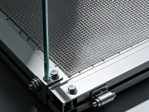
A frameless stencil consists of a thin metal foil, typically stainless steel or nickel, tensioned directly onto the printer using a separate mounting system rather than a permanent frame. This design reduces storage space and allows quick changes between jobs. In high-mix environments, the approach supports faster turnaround without the expense of multiple framed stencils. Industry standards such as IPC-7525 provide guidelines for stencil thickness and aperture design that apply equally to frameless formats. When used correctly, frameless stencils help achieve reliable paste release on fine-pitch components while keeping overall process costs under control.
Technical Principles Behind Frameless Stencil Performance
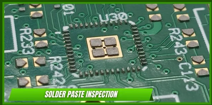
Frameless stencils rely on uniform tension applied across the foil to maintain flatness during printing. Any deviation in tension or support can cause the stencil to flex, leading to gaps between the stencil and the printed circuit board. These gaps allow solder paste to squeeze under the stencil edges and create bridges between adjacent pads. Insufficient solder often results from poor paste release caused by inadequate aperture aspect ratios or surface finish on the stencil foil. Regular inspection of stencil condition becomes essential because even minor dents or scratches alter paste volume. Engineers evaluate these factors by measuring actual paste deposits with automated optical inspection systems after the print step.
Related Reading: Framed vs. Frameless Stencils: Understanding the Pros and Cons for SMT Assembly
Common Causes of Stencil Misalignment
Stencil misalignment occurs when the stencil apertures do not register accurately with the PCB pads. Contributing factors include thermal expansion of the board material, fixture wear, and variations in board thickness. Warpage in the printed circuit board further complicates contact, especially on larger panels. Operators must verify fiducial alignment and confirm that the printer’s vision system has correctly identified both board and stencil marks. Consistent machine calibration and periodic verification of support pins reduce the likelihood of offset prints that produce tombstones or insufficient solder joints.
Addressing Solder Bridging and Insufficient Solder Deposits
Solder bridging typically stems from excessive paste volume or poor stencil release on closely spaced pads. Adjusting aperture reductions according to component pitch and following recommended aspect ratios helps control deposit size. Insufficient solder often appears when the stencil surface becomes contaminated or when paste viscosity changes due to temperature fluctuations in the production area. Monitoring ambient conditions and using fresh paste batches supports consistent volume transfer. In both cases, reviewing the print parameters and stencil condition before production runs prevents defects from propagating through reflow.
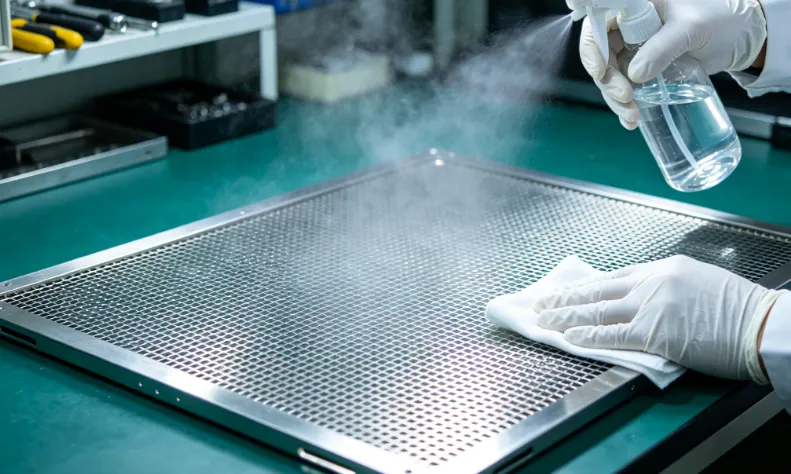
Best Practices for Stencil Cleaning and Maintenance
Effective stencil cleaning removes dried paste from apertures and the underside surface to restore print quality. Manual wiping with lint-free cloths and approved solvents works for light buildup, while ultrasonic or automated cleaning systems handle heavier residues. Cleaning frequency depends on paste type and production volume; many lines schedule cleaning after every 5 to 10 prints for fine-pitch work. Proper storage of the stencil in a flat, protected environment prevents warping when not in use. Following these steps extends stencil life and maintains deposition accuracy across multiple jobs.
Related Reading: The Ultimate Guide to Stencil Cleaning: Ensuring Consistent Solder Paste Deposition
Troubleshooting Workflow for Frameless Stencil Issues
When defects appear, start by examining the most recent prints with automated optical inspection data to identify patterns. Compare actual paste volumes against target values to distinguish between misalignment and release problems. Next, inspect the stencil foil under magnification for damage or residue. Adjust printer settings such as squeegee pressure and speed only after confirming the stencil and board are properly supported. Document each adjustment and re-verify results on subsequent prints to build a reliable process history.
Conclusion
Frameless stencils offer clear advantages in flexibility and cost for many PCB assembly operations, yet they require disciplined attention to alignment, paste release, and cleaning routines. By applying structured troubleshooting steps and adhering to established process controls, engineering teams can minimize common defects such as stencil misalignment, solder bridging, and insufficient solder. Consistent maintenance practices further support long-term stencil performance and overall assembly yield.
FAQs
Q1: How can operators reduce frameless stencil problems during high-mix production?
A1: Regular verification of stencil tension and fiducial alignment, combined with scheduled cleaning cycles, helps maintain registration accuracy and prevents paste buildup that leads to bridging or insufficient deposits.
Q2: What steps minimize stencil misalignment on warped PCBs?
A2: Support pins should be adjusted to match board topography, and vision system calibration should be confirmed before each run. These actions compensate for warpage and keep apertures properly registered with the pads.
Q3: Why does solder bridging occur more frequently with frameless stencils?
A3: Reduced frame rigidity can allow slight flexing if tension is uneven, creating gaps that permit paste to flow between pads. Proper aperture design and consistent cleaning reduce this risk.
Q4: How often should stencil cleaning occur to avoid insufficient solder?
A4: Cleaning intervals depend on paste type and print volume, but many processes benefit from inspection and cleaning after every five to ten prints to ensure clear apertures and consistent paste release.
References
IPC-7525 - Stencil Design Guidelines. IPC, 2023
IPC-A-610H - Acceptability of Electronic Assemblies. IPC, 2020
J-STD-001H - Requirements for Soldered Electrical and Electronic Assemblies. IPC, 2020


