 ALLPCB


Introduction
Stencil thickness plays a central role in surface mount technology processes where solder paste must be deposited accurately onto printed circuit boards. Engineers and assembly teams rely on proper thickness selection to achieve consistent paste volumes that support reliable electrical connections after reflow soldering. When thickness is chosen correctly, the resulting solder joints meet quality expectations for strength and conductivity while minimizing defects that could affect long term performance. This guide examines the factors that influence stencil thickness decisions and provides practical steps for achieving better outcomes in PCB assembly. The discussion draws on established engineering practices to help professionals optimize their processes without unnecessary trial and error.
What Is Stencil Thickness and Why It Matters
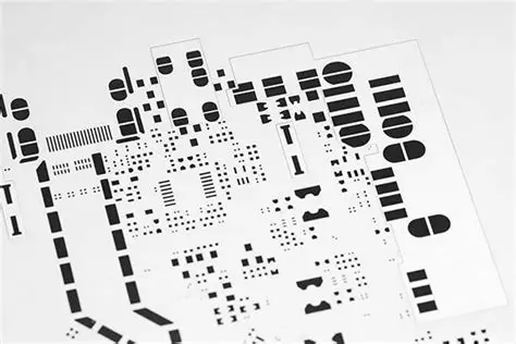
Stencil thickness refers to the depth of the metal foil used to create openings that control how much solder paste transfers onto board pads during printing. This dimension directly determines the volume of paste applied, which in turn influences the amount of solder available to form joints during reflow soldering. In high volume manufacturing environments, even small variations in thickness can lead to differences in joint formation that affect both yield and reliability. Proper selection supports the goals of SMT stencil thickness selection by balancing paste release efficiency with the need for adequate material on each pad. Industry professionals recognize that stencil thickness for reflow soldering must align with component types and board layout to avoid common issues such as insufficient fillet or excess material that causes bridging. 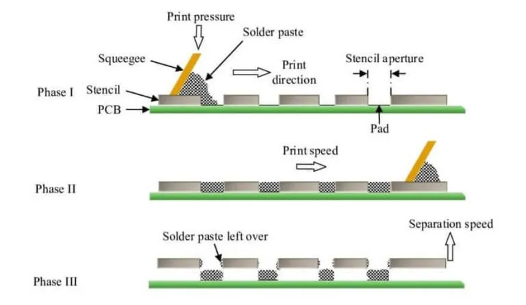
Technical Principles and Mechanisms
The mechanism behind stencil thickness involves the relationship between foil depth and the area ratio of each aperture, which governs how cleanly paste releases onto the board surface. Thicker foils generally allow greater paste volume but can reduce release efficiency when apertures are small relative to the thickness, leading to incomplete deposits. Conversely, thinner foils improve release for fine pitch components yet may not supply enough material for larger pads that require stronger joints. These interactions directly affect solder joint quality because the final fillet height and shape depend on the initial paste volume transferred. Engineers evaluate these principles by considering board warpage, component lead geometry, and paste rheology together rather than treating thickness as an isolated variable.
Related Reading: Step Stencil Thickness: How to Determine the Ideal Value for Your PCB
Practical Solutions and Best Practices
Selection begins with reviewing the component mix and pad designs on the assembly to determine an appropriate starting thickness that supports both fine and coarse features. Calculation methods typically combine aperture dimensions with desired paste volume targets, allowing teams to adjust thickness iteratively based on test prints and inspection results. Troubleshooting often focuses on symptoms such as poor paste release or uneven deposits, which can be addressed by modifying thickness in combination with aperture shape or surface finish. Teams following established guidelines achieve more consistent outcomes by documenting thickness choices alongside other process parameters for future reference. Regular verification through visual inspection and automated optical systems helps confirm that the chosen thickness continues to deliver acceptable joint formation across production runs. 
Troubleshooting Insights for Assembly Teams
Common challenges arise when stencil thickness does not match the demands of mixed technology boards, resulting in either starved or overfilled joints after reflow. In such cases, teams examine the printing process for signs of paste smearing or incomplete transfer and then evaluate whether a change in thickness would improve volume control without introducing new defects. Practical adjustments often involve creating test stencils with incremental thickness variations to observe real world performance on the specific board design. This approach reduces downtime by identifying the optimal balance between paste deposition and release characteristics before full scale production begins. Documentation of these trials supports ongoing process refinement and helps new team members understand the reasoning behind thickness decisions.
Related Reading: The Impact of Stencil Thickness on Solder Joint Quality: A Detailed Analysis
Conclusion
Stencil thickness remains a fundamental variable that influences the success of PCB assembly through its effect on paste volume and final solder joint formation. By applying structured selection methods and addressing issues through targeted troubleshooting, engineers can improve yield and reliability while meeting the requirements of modern SMT processes. Consistent attention to thickness alongside other process elements supports high quality outcomes across diverse board configurations. The principles outlined here provide a foundation for informed decisions that align with industry expectations for performance and repeatability.
FAQs
Q1: How does stencil thickness impact solder joint quality in PCB assembly?
A1: Stencil thickness directly controls the volume of solder paste deposited on pads, which determines the final shape and strength of joints formed during reflow soldering. Incorrect thickness can produce insufficient material leading to weak connections or excess paste that causes bridging and shorts. Engineers evaluate this relationship during SMT stencil thickness selection to ensure joints meet acceptance criteria for mechanical and electrical performance. Proper choices reduce defects and support consistent results across production batches.
Q2: What factors guide SMT stencil thickness selection for different components?
A2: Component pitch, pad size, and board surface conditions all influence the thickness chosen to achieve reliable paste transfer. Thinner foils often suit fine pitch devices where release efficiency matters most, while slightly thicker options help larger components receive adequate material. Teams combine these considerations with stencil thickness calculation techniques to arrive at a value that balances multiple requirements on a single board. This practical approach minimizes the need for extensive rework after reflow.
Q3: Can stencil thickness calculation improve results in reflow soldering processes?
A3: Calculation methods help predict paste volume based on aperture dimensions and foil depth, allowing adjustments before production printing begins. By incorporating board layout details and component specifications, engineers can select a thickness that supports uniform deposits and reduces common reflow defects. This step forms part of a broader PCB stencil thickness guide that emphasizes verification through test prints rather than assumptions. Consistent application leads to better joint quality and higher first pass yields.
Q4: Why is stencil thickness for reflow soldering critical in mixed technology assemblies?
A4: Mixed boards contain both small and large components that require different paste volumes for optimal joint formation. A single thickness must accommodate these variations without causing starved joints on one type or excess material on another. Practical troubleshooting often starts with thickness review when defects appear after reflow, guiding targeted adjustments that restore process stability. This focus helps maintain quality across complex designs without unnecessary equipment changes.


