 ALLPCB


Introduction
In high-speed PCB design, maintaining signal integrity is crucial as data rates continue to increase. Through-hole vias serve as essential interconnects between layers, but they introduce parasitic effects that can degrade signal quality. Engineers must understand through-hole via inductance and through-hole via capacitance to optimize performance. The via stub effect further complicates designs by causing reflections and resonances. This guide explores these challenges and provides structured strategies for effective via design. By addressing these elements, designers can ensure reliable signal transmission in demanding applications.
Understanding Through-Hole Vias and Their Role in PCBs
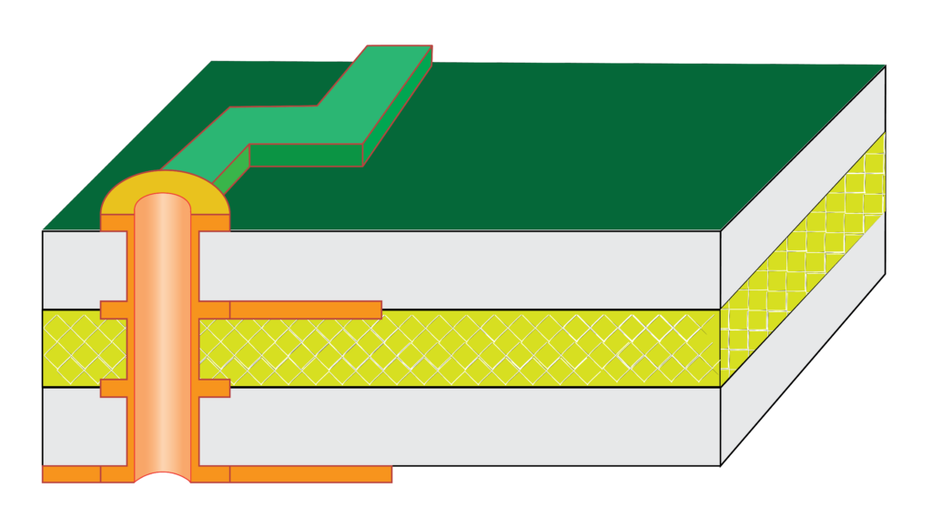
Through-hole vias are plated holes that extend fully through the PCB stackup, connecting traces on multiple layers. They offer robust mechanical strength and are suitable for components requiring high reliability. However, in high-speed environments, these vias create discontinuities in the transmission line. Signal integrity suffers from mismatches in characteristic impedance caused by the via geometry. Proper design minimizes these issues while adhering to fabrication capabilities. IPC-2221 provides foundational guidelines for via dimensions and spacing to support electrical performance.
The primary concerns arise from the via's electrical properties interacting with fast-rising signals. Rise times in the picosecond range amplify parasitic effects, leading to overshoot, ringing, and attenuation. Designers evaluate via placement relative to signal paths to predict impacts. Layer count and board thickness influence via length, exacerbating problems in thick stackups. Balancing connectivity needs with signal demands requires careful planning from the outset.
Key Electrical Characteristics: Inductance and Capacitance
Through-hole via inductance stems from the current loop formed by the signal path through the barrel and return via ground planes. Longer vias increase inductance, which slows signal rise times and causes voltage droop. Approximate inductance scales with via height and inversely with diameter, following established engineering models. In differential pairs, unbalanced via inductance introduces skew, degrading eye diagrams. Engineers model this using field solvers to quantify effects before layout finalization.
Through-hole via capacitance arises from the interaction between the via barrel and surrounding planes or antipads. The capacitance value depends on dielectric constant, via diameter, and antipad size. Excessive capacitance leads to signal broadening and inter-symbol interference. Optimization involves adjusting antipad dimensions to control coupling without compromising manufacturability. These parasitics combine to form a lumped LC network that resonates at specific frequencies.
Precise control requires simulation of the via transition as a discontinuity in the impedance profile. Return loss increases when the via impedance deviates significantly from the trace. Ground planes adjacent to the via reduce effective inductance by shortening return paths. Capacitance management ensures smooth energy transfer across layers.
The Via Stub Effect and Its Impact on Signal Integrity
The via stub effect occurs when the unused portion of a through-hole via beyond the target layer acts as an open-ended transmission line. At frequencies where the stub length approaches a quarter wavelength, it reflects signals back, creating nulls in the frequency response. This degrades insertion loss and introduces severe signal integrity issues in high-speed PCB design. Stub resonances typically manifest above several gigahertz, depending on board thickness and dielectric properties.
Longer stubs in multilayer boards amplify the problem, as total via length exceeds signal transition depth. Reflections superimpose on the primary signal, causing distortion and bit errors. Time-domain reflectometry reveals these effects through ringing in eye patterns. Mitigation strategies focus on shortening or eliminating stubs to preserve bandwidth.
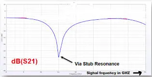
Engineers calculate stub quarter-wave frequency using velocity of propagation in the dielectric. For FR-4 materials, this falls in the multi-GHz range for typical stub lengths. Pre-layout analysis identifies critical nets prone to stub dominance. Post-simulation verification confirms acceptable return loss margins.
Design Parameters Influencing Via Performance
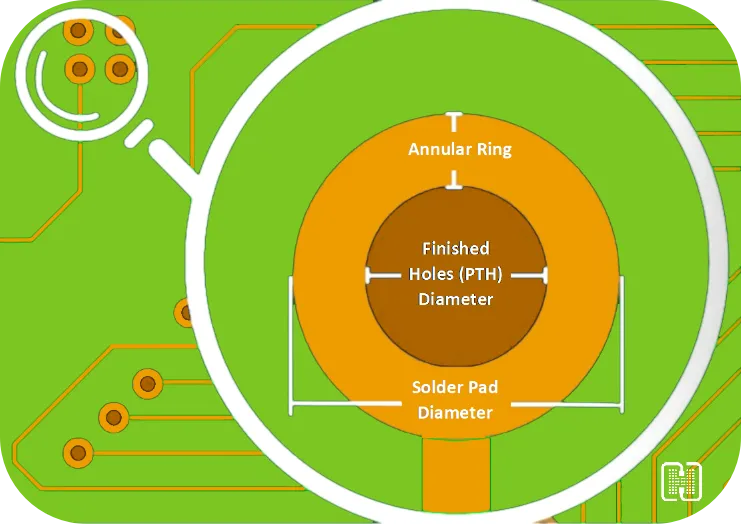
Via diameter selection balances inductance reduction with drill feasibility and annular ring requirements. Smaller diameters lower inductance but demand precise fabrication tolerances. IPC-6012E specifies minimum annular rings for reliability under thermal stress. Aspect ratios, defined as board thickness over drill diameter, limit plating uniformity. Optimal ratios prevent voids that could increase resistance and inductance.
Antipad and pad sizing control capacitance and impedance continuity. Larger antipads reduce capacitance but may weaken plane coupling. Trace-to-via transitions require fanout patterns to maintain 50-ohm impedance. Pairing signal vias with nearby ground vias forms return paths, minimizing loop inductance.
Stackup planning positions signal layers closer to reference planes to shorten via stubs. Thinner dielectrics enable shorter vias overall. Routing high-speed signals on inner layers reduces stub exposure.
Best Practices for Through-Hole Via Design in High-Speed PCBs
Minimize via count on critical nets by optimizing layer usage and component placement. Use wider traces feeding into larger vias to ease impedance steps. Simulate S-parameters for via arrays in dense routing. Backdrilling removes stub ends, though it adds cost and tolerance challenges. Controlled depth drilling ensures clean removal without damaging inner connections.
Implement via-in-pad techniques for dense designs, filling with conductive epoxy if needed. Stagger via pairs for differential signals to balance parasitics. Reference planes must be stitched with vias to provide low-inductance returns. Avoid splitting planes under high-speed vias to prevent return path detours.
For power vias, multiple parallel vias distribute current and reduce effective inductance. Thermal relief patterns aid soldering without compromising electrical paths. Final design review includes DFM checks for drill sizes and plating.
Troubleshooting Common Via-Related Signal Integrity Issues
Excessive ringing often traces to high via inductance; confirm with TDR measurements. Deep insertion loss nulls indicate stub resonances; adjust routing or backdrill. Skew in differential pairs stems from asymmetric via placement; symmetrize layouts. Crosstalk rises with poor ground referencing; add shielding vias.
Simulation discrepancies versus hardware point to unmodeled parasitics; refine models with measured dielectric constants. Fabrication variations like plating thickness alter inductance; specify tight tolerances. Iterative prototyping refines designs for production.
Conclusion
Through-hole via design demands attention to inductance, capacitance, and stub effects for robust signal integrity. Strategic sizing, placement, and processing techniques mitigate parasitics effectively. Adhering to standards ensures manufacturability alongside performance. High-speed PCB design benefits from simulation-driven approaches. Implementing these principles yields reliable boards ready for gigabit speeds.
FAQs
Q1: What causes the via stub effect in through-hole vias?
A1: The via stub effect arises from the unused barrel length acting as a quarter-wave resonator, reflecting signals at specific frequencies. This disrupts signal integrity in high-speed PCB design by creating insertion loss nulls. Mitigation includes backdrilling or using blind vias to shorten stubs. Proper stackup planning minimizes stub lengths from the start.
Q2: How does through-hole via inductance impact high-speed signals?
A2: Through-hole via inductance slows rise times and introduces voltage droop, especially in long vias. It causes impedance discontinuities leading to overshoot and EMI. Reducing via length and diameter lowers inductance. Pairing with ground vias shortens return paths for better performance.
Q3: Why is through-hole via capacitance important for signal integrity?
A3: Through-hole via capacitance broadens pulses and causes inter-symbol interference due to energy storage. Antipad sizing controls this parasitic to match trace impedance. Excessive capacitance degrades eye height in high-speed designs. Balanced design maintains clean signal transitions.
Q4: What are best practices to optimize vias for signal integrity?
A4: Select via diameters per fabrication limits while minimizing length. Use backdrilling for critical nets to eliminate stubs. Simulate parasitics and ensure reference planes. Follow IPC guidelines for annular rings and spacing.
References
IPC-2221B — Generic Standard on Printed Board Design. IPC, 2012
IPC-6012E — Qualification and Performance Specification for Rigid Printed Boards. IPC, 2017
J-STD-001H — Requirements for Soldered Electrical and Electronic Assemblies. IPC, 2018


