 ALLPCB


Introduction
In high-speed PCB design, achieving precise PCB impedance control is essential for maintaining signal integrity. Line width tolerance directly influences the performance of controlled impedance traces, where even small variations can lead to reflections, crosstalk, or signal degradation. Electrical engineers must master these tolerances to ensure reliable operation in applications like RF circuits, data buses, and telecommunications equipment. This article explores the critical relationship between line width tolerance and impedance, focusing on microstrip impedance and stripline impedance structures. By understanding manufacturing variations and design strategies, engineers can optimize trace geometries using tools like a trace width calculator. Proper management of these factors aligns with industry standards such as IPC-2221, enabling robust designs that meet performance specifications.
Line width tolerance refers to the allowable deviation in trace width during fabrication, typically influenced by etching processes and material properties. For controlled impedance traces, tighter tolerances are often required to hit target impedance values, such as 50 ohms or 100 ohms differential. Engineers face challenges from dielectric variations and copper thickness inconsistencies, which compound line width effects. This guide provides structured insights into principles, best practices, and troubleshooting, empowering designers to specify requirements effectively.
What Is Line Width Tolerance and Why It Matters for PCB Impedance Control
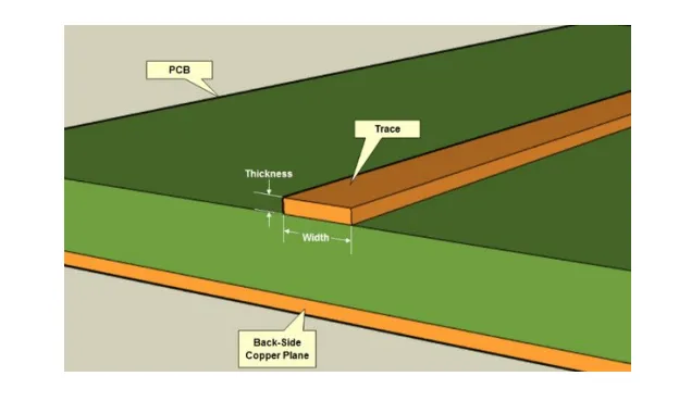
Line width tolerance defines the permissible variation between the designed trace width and the fabricated dimension, expressed as a percentage or absolute value. In PCB manufacturing, this tolerance arises from etching undercuts, plating buildup, and exposure alignment. For standard traces, tolerances may range widely, but controlled impedance traces demand precision to prevent impedance mismatches. A controlled impedance trace maintains a consistent characteristic impedance along its length, crucial for high-frequency signals where wavelength approaches trace dimensions.
The relevance intensifies in modern electronics, where data rates exceed gigabits per second. Impedance discontinuities from poor line width control cause signal reflections, quantified by return loss in decibels. Engineers using a trace width calculator must account for these tolerances early in the design phase to predict real-world performance. Factory-driven insights emphasize that tolerances tighter than standard levels reduce yield risks and enhance reliability. Ultimately, mastering line width tolerance ensures PCB impedance control aligns with application demands, minimizing redesign iterations.
In multilayer boards, inner layer tolerances differ from outer layers due to lamination pressures and foil types. External traces experience more exposure variability, while embedded structures benefit from symmetric dielectrics. Standards like IPC-A-600 provide acceptability criteria for conductor widths, guiding quality control. Neglecting these aspects leads to costly respins, underscoring the need for proactive tolerance management.
Technical Principles of Microstrip and Stripline Impedance
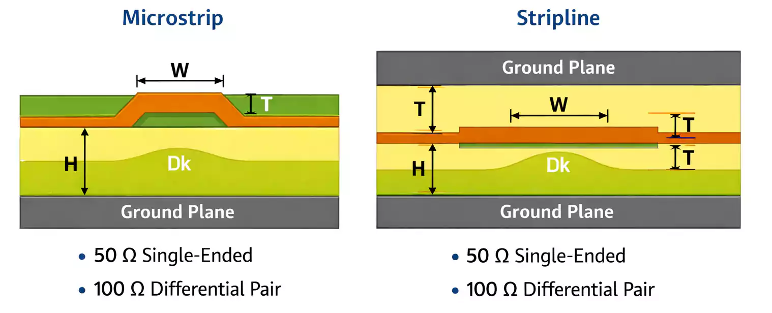
Microstrip impedance depends on trace width, dielectric height, and substrate properties, following transmission line theory. The characteristic impedance Z0 decreases as trace width increases, due to reduced inductance and increased capacitance. Engineers calculate microstrip impedance using field solver models or approximate equations, inputting parameters into a trace width calculator for iterative optimization. Dielectric constant variations amplify width tolerance effects, as effective epsilon influences wave propagation.
Stripline impedance, embedded between ground planes, offers better shielding but requires narrower traces for equivalent Z0 compared to microstrip. Symmetric stripline maintains uniform fields, making it less sensitive to width deviations in centered configurations. However, asymmetric stripline demands precise width control to avoid mode conversion. Both structures highlight how a 10% width change can shift impedance by several ohms, critical for broadband matching.
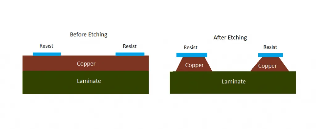
Fabrication processes etch traces from copper foil, where isotropic etching causes undercuts proportional to foil thickness. Panel-level processes introduce cumulative errors across large arrays. Copper weight, from 1 oz to 2 oz per square foot, scales tolerance impacts, as thicker foils yield larger absolute deviations. Dielectric thickness tolerance interacts multiplicatively, per IPC-6012 performance specifications, necessitating stackup verification.
Field distribution in microstrip exposes one side to air, lowering effective dielectric constant and widening required traces. Stripline fully embeds the trace, increasing capacitance and narrowing widths for the same Z0. Engineers model these using quasi-TEM approximations, validating with time-domain reflectometry post-fabrication. Understanding these principles allows prediction of tolerance-induced variations during design reviews.
Factors Influencing Line Width Tolerance in Controlled Impedance Traces
Several manufacturing variables dictate line width tolerance outcomes. Etching chemistry and time control undercut, typically symmetric around the trace center. Plating for vias adds lateral growth, narrowing spaces between controlled impedance traces. Dielectric prepreg flow during lamination can shift inner layers, altering effective heights for stripline impedance.
Material selection plays a key role, with low-loss dielectrics enabling high-frequency PCB impedance control but introducing variability in resin content. Copper surface roughness affects skin effect losses, indirectly influencing impedance at gigahertz frequencies. Engineers must specify foil types, such as electrodeposited or rolled annealed, to predict tolerance bands.
Environmental factors during fabrication, like temperature and humidity, impact photoresist adhesion and development. Automated optical inspection verifies widths post-etch, but human oversight ensures compliance. Stackup asymmetry exacerbates tolerances in multilayer boards, requiring symmetric builds for stripline consistency.
Best Practices for Optimal Line Width Tolerance and PCB Impedance Control
Start with accurate stackup definition, specifying dielectric thicknesses and copper weights per layer. Use a trace width calculator to nominate widths achieving target impedances, incorporating nominal tolerances. Allocate margins by designing traces slightly wider than calculated, compensating for etch back. Collaborate with fabricators early to confirm capability matrices for impedance tolerance.
Implement design rules enforcing minimum spacings between controlled impedance traces, preventing crosstalk. Route high-speed nets on dedicated layers with ground references, optimizing microstrip impedance. For stripline, ensure ground plane continuity to minimize field fringing. Simulate impedance profiles using 2D field solvers, validating against measured TDR data.
During Gerber review, overlay impedance coupons for test structures per industry guidelines. Specify impedance targets with tolerances, such as ±10%, on fabrication drawings. Post-lamination, perform cross-section analysis to verify heights before final etch. These steps align with IPC-2221 design standards, enhancing manufacturability.
Employ length-matching for differential pairs, maintaining edge coupling via consistent widths. Avoid vias in critical segments or use back-drilling to preserve impedance. For high-density interconnects, finer lines demand advanced imaging for tolerance control. Regular process audits refine capabilities over production runs.
Troubleshooting Common Line Width Tolerance Issues
Deviations often manifest as impedance mismatches detected via TDR or VNA measurements. Narrower traces increase Z0, causing overshoot in eye diagrams. Wider traces lower Z0, risking ringing. Cross-section microscopy reveals etch asymmetry or plating excesses.
If tolerances exceed expectations, review exposure dosage and developer strength. Lamination voids shift dielectrics, altering stripline impedance; X-ray inspection identifies these. Recalculate using adjusted parameters in a trace width calculator for redesigns. Iterative fab runs with test vehicles refine processes.
Fabrication feedback loops, including coupon data, pinpoint systemic issues like panel warp affecting alignment. Address via fixture clamping or thinner cores. Consistent documentation ensures traceability.
Conclusion
Mastering line width tolerance is pivotal for effective PCB impedance control, directly impacting controlled impedance trace performance. By grasping microstrip impedance and stripline impedance principles, engineers can leverage trace width calculators for precise designs. Adopting best practices, from stackup planning to verification, mitigates manufacturing variations. Alignment with standards like IPC-6012 ensures quality outcomes. Prioritizing these elements yields reliable high-speed PCBs, reducing risks and accelerating time-to-market.
FAQs
Q1: What role does line width tolerance play in PCB impedance control?
A1: Line width tolerance determines how closely fabricated traces match designed dimensions, directly affecting characteristic impedance. Variations alter inductance and capacitance, leading to mismatches in controlled impedance traces. Engineers use trace width calculators to predict and compensate for these effects, ensuring signal integrity. Tighter tolerances, often ±10%, are standard for high-speed applications per IPC guidelines.
Q2: How does microstrip impedance differ from stripline impedance regarding trace width?
A2: Microstrip requires wider traces than stripline for the same impedance due to partial air dielectric, increasing sensitivity to width tolerances. Stripline's full embedding provides shielding but demands precise centering. Both benefit from controlled dielectric heights to stabilize PCB impedance control. Design tools model these differences for optimal routing.
Q3: Why use a trace width calculator for controlled impedance traces?
A3: A trace width calculator computes optimal widths based on stackup parameters, dielectric constants, and target impedances. It accounts for manufacturing tolerances, preventing post-fab surprises. For microstrip and stripline structures, iterative calculations refine designs. This tool integrates seamlessly into workflows, enhancing accuracy for high-frequency PCB impedance control.
Q4: What are best practices for specifying line width tolerance in PCB manufacturing?
A4: Specify tolerances explicitly on drawings, targeting ±10% for impedance-critical nets. Include stackup details and test coupons. Verify via cross-sections and TDR. Collaborate on process capabilities to align design with fabrication limits. These steps ensure reliable controlled impedance traces across production.
References
IPC-2221B — Generic Standard on Printed Board Design. IPC, 2012
IPC-6012E — Qualification and Performance Specification for Rigid Printed Boards. IPC, 2015
IPC-A-600K — Acceptability of Printed Boards. IPC, 2020


