ALLPCB


If you’re wondering how signal layer thickness affects PCB performance, the answer lies in its influence on signal integrity, current carrying capacity, and manufacturing precision. Simply put, the thickness of the signal layer—often determined by the copper weight—plays a critical role in how well signals travel through a printed circuit board (PCB), how much current the traces can handle, and how accurately the board can be produced. In this detailed blog post, we’ll dive deep into the nuances of signal layer thickness, explore related factors like PCB trace width, signal layer current carrying capacity, signal layer etching tolerances, and signal layer copper weight, and provide practical insights for optimizing your PCB designs.
Introduction to Signal Layer Thickness in PCB Design
Printed circuit boards are the backbone of modern electronics, and every layer within them serves a specific purpose. The signal layer, where electrical signals travel through copper traces, is one of the most critical components. The thickness of this layer, often measured in terms of copper weight (e.g., 1 oz/ft2, 2 oz/ft2), directly impacts the board’s performance. A thicker signal layer can carry more current and reduce resistance, but it may also affect signal speed and manufacturing costs. On the other hand, a thinner layer might be ideal for high-speed signals but could struggle with higher currents.
Understanding the balance between these factors is essential for engineers and designers. Whether you’re working on a high-speed communication device or a power-heavy industrial application, the signal layer thickness can make or break your design. Let’s break down the key aspects of how this parameter influences PCB performance.
What Is Signal Layer Thickness and Why Does It Matter?
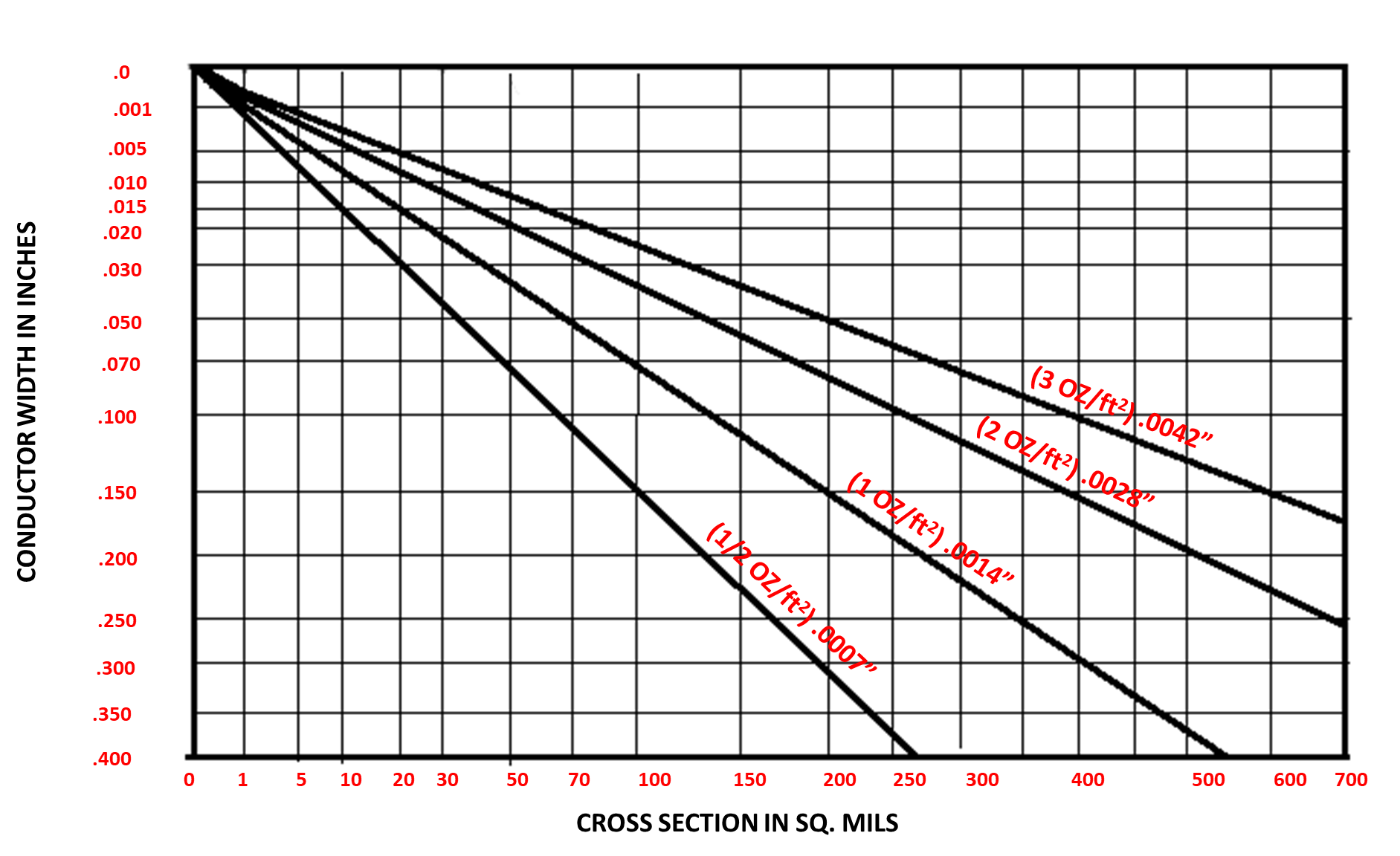
Signal layer thickness refers to the amount of copper used in the conductive layer of a PCB, typically measured in ounces per square foot (oz/ft2). For example, 1 oz/ft2 corresponds to a thickness of about 1.4 mils (0.035 mm), while 2 oz/ft2 is roughly 2.8 mils (0.07 mm). This thickness determines several critical properties of the PCB, including resistance, current carrying capacity, and signal integrity.
Why does this matter? In high-speed designs, thinner layers reduce parasitic capacitance and improve signal propagation speed, which is crucial for maintaining signal integrity at frequencies above 10 GHz. However, in power applications, thicker layers are preferred to handle higher currents without overheating or voltage drops. Striking the right balance is key, and it starts with understanding the specific needs of your project.
The Relationship Between Signal Layer Thickness and Signal Integrity
Signal integrity is the ability of an electrical signal to maintain its shape and timing as it travels through the PCB. Factors like reflections, crosstalk, and electromagnetic interference (EMI) can degrade signal quality, and signal layer thickness plays a significant role in managing these issues.
For high-speed signals, a thinner copper layer is often better. Why? Thinner layers result in narrower traces for a given impedance (e.g., 50 ohms, a common standard for high-speed signals), which reduces the distance signals need to travel across adjacent layers or components, minimizing crosstalk. Additionally, thinner layers have less parasitic capacitance, allowing signals to propagate faster. For instance, in a design operating at 5 GHz, a 0.5 oz/ft2 copper layer might be ideal to maintain signal clarity.
However, thinner layers can introduce challenges. They have higher resistance, which can lead to signal loss over long traces. If not carefully managed, this can distort the signal waveform, especially in analog or high-frequency digital applications. Therefore, designers must weigh the benefits of thinner layers against potential drawbacks.
 "
"
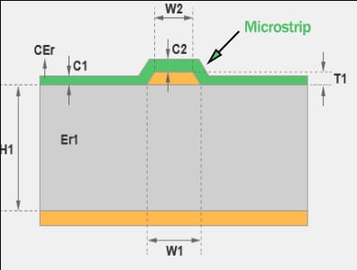
PCB Trace Width and Its Connection to Signal Layer Thickness
Another critical factor tied to signal layer thickness is PCB trace width. Trace width refers to the physical width of the copper paths on the signal layer that carry electrical signals. The thickness of the copper layer directly influences the trace width required to achieve a specific impedance or current capacity.
For example, to maintain a 50-ohm impedance in a high-speed design, a thinner copper layer (e.g., 0.5 oz/ft2) requires a narrower trace width compared to a thicker layer (e.g., 2 oz/ft2). This is because impedance is a function of both the trace geometry and the dielectric properties of the PCB material. A narrower trace on a thinner layer can help reduce crosstalk but may also increase resistance, leading to potential signal attenuation.
In contrast, wider traces are often used with thicker copper layers for power distribution, as they can handle more current without overheating. Tools like impedance calculators can help determine the optimal trace width for a given copper thickness, ensuring that your design meets both signal integrity and thermal requirements.
Signal Layer Current Carrying Capacity: How Thickness Plays a Role
The signal layer current carrying capacity is a measure of how much current a trace can handle without overheating or failing. This capacity is directly proportional to the copper thickness and trace width. Thicker copper layers can carry more current because they have lower resistance and can dissipate heat more effectively.
For instance, a 1 oz/ft2 copper layer with a trace width of 10 mils might safely carry around 1 ampere of current under typical conditions. Doubling the copper thickness to 2 oz/ft2 could increase the current capacity to approximately 2 amperes for the same trace width, assuming proper thermal management. These values are based on standard industry guidelines, such as those from the IPC-2221 standard, which provides formulas for calculating current capacity based on trace dimensions and temperature rise.
In power-heavy applications, such as motor controllers or power supplies, opting for a thicker signal layer is often necessary to prevent overheating and ensure reliability. However, thicker layers increase manufacturing costs and may not be suitable for high-density designs where space is limited. Balancing current needs with design constraints is a critical consideration.
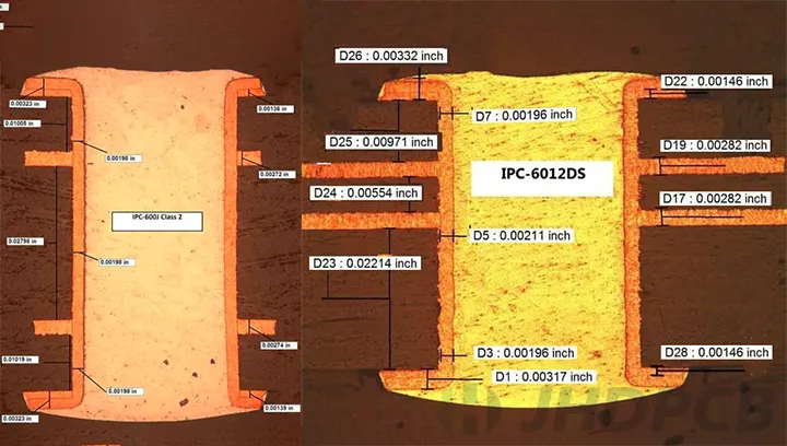
Signal Layer Etching Tolerances: Precision in Manufacturing
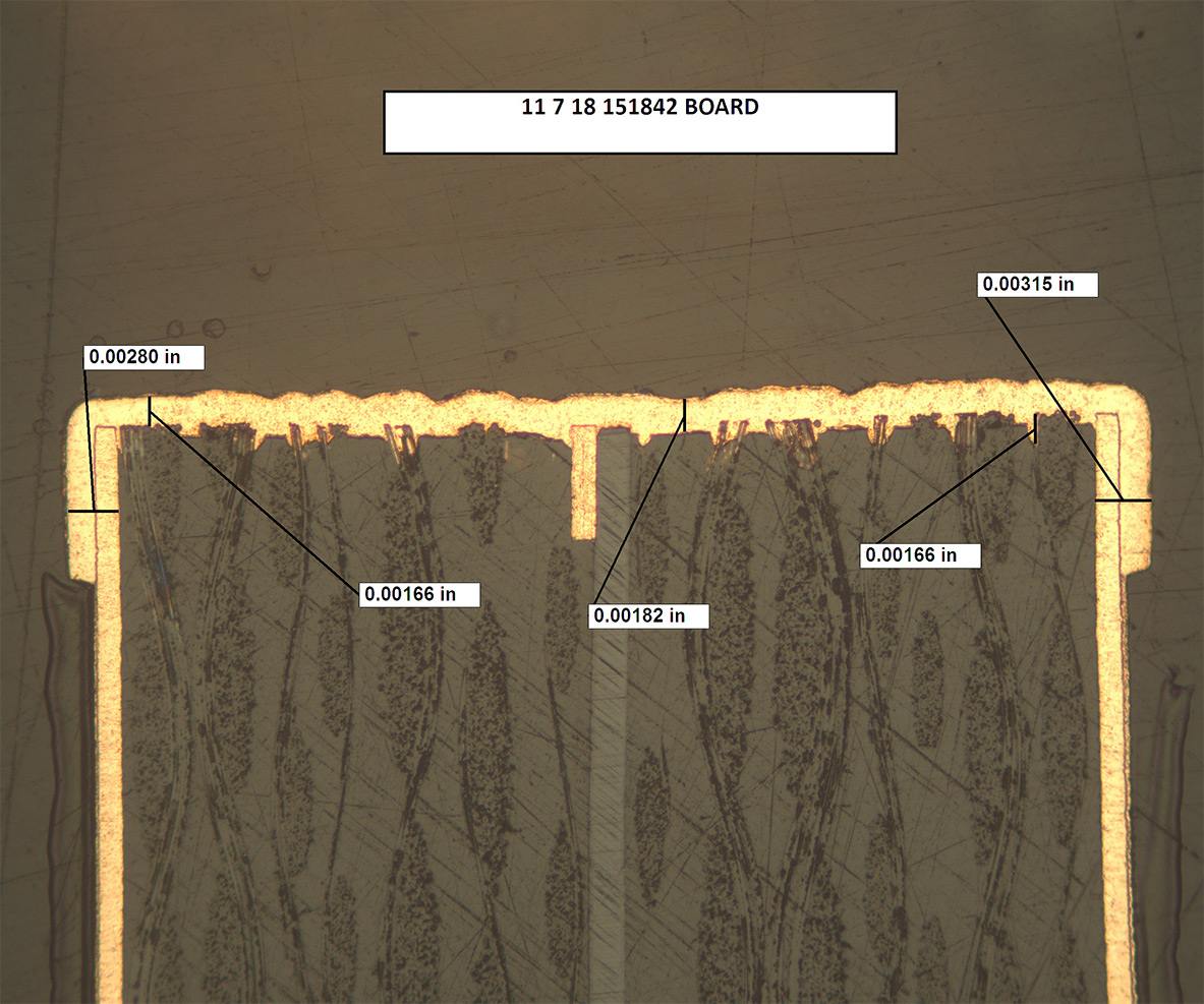
Manufacturing precision is another area where signal layer etching tolerances come into play, and this is influenced by the copper thickness. Etching is the process of removing unwanted copper from the PCB to create the desired trace patterns. The thicker the copper layer, the more challenging it is to achieve tight tolerances during etching.
For example, a 1 oz/ft2 copper layer can typically be etched with a tolerance of ±1 mil for trace widths. However, with a 3 oz/ft2 layer, the tolerance might widen to ±2 mils due to the increased difficulty of controlling the etching process on thicker material. This can lead to variations in trace width, which in turn affect impedance and signal integrity, especially in high-speed designs.
Designers must account for these tolerances when specifying copper thickness and trace dimensions. Working closely with your PCB manufacturer to understand their etching capabilities can help ensure that your design is manufacturable without compromising performance. For high-precision applications, a thinner copper layer might be preferable to achieve tighter tolerances, even if it means sacrificing some current carrying capacity.
The Role of Signal Layer Copper Weight in PCB Design
The term signal layer copper weight is often used interchangeably with thickness, as it directly correlates to the amount of copper on the layer. Common copper weights in PCB design range from 0.5 oz/ft2 to 4 oz/ft2, with 1 oz/ft2 being the industry standard for most general-purpose applications.
Choosing the right copper weight involves balancing several factors:
- Cost: Thicker copper weights are more expensive due to increased material and processing costs.
- Performance: Heavier copper weights reduce resistance and improve current handling, but they can negatively impact high-speed signal performance due to increased capacitance.
- Manufacturability: As mentioned earlier, thicker copper is harder to etch precisely, which can affect trace accuracy.
For example, a 2 oz/ft2 copper weight might be ideal for a power distribution board where current handling is critical. However, for a high-frequency RF design, a 0.5 oz/ft2 weight could be better to minimize signal loss and maintain impedance control. Understanding the specific demands of your application is essential for selecting the appropriate copper weight.
Practical Design Tips for Optimizing Signal Layer Thickness
Now that we’ve covered the technical aspects of signal layer thickness, let’s look at some actionable tips to optimize your PCB design:
- Match Thickness to Application: Use thinner layers (e.g., 0.5–1 oz/ft2) for high-speed signals and thicker layers (e.g., 2–3 oz/ft2) for power delivery.
- Calculate Impedance Early: Use impedance calculation tools to determine the required trace width and layer thickness for your target impedance (e.g., 50 ohms).
- Consider Thermal Management: Thicker layers dissipate heat better, so factor in thermal requirements when selecting copper weight for high-current designs.
- Consult Manufacturing Guidelines: Check with your PCB fabricator about their etching tolerances and capabilities for different copper weights to avoid design issues.
- Simulate Before Prototyping: Use simulation software to model signal integrity and current flow for different layer thicknesses, ensuring your design performs as expected.
Conclusion: Balancing Signal Layer Thickness for Optimal PCB Performance
The signal layer thickness is a fundamental parameter that influences nearly every aspect of PCB performance, from signal integrity to current carrying capacity. By carefully considering factors like PCB trace width, signal layer current carrying capacity, signal layer etching tolerances, and signal layer copper weight, designers can create boards that meet the specific needs of their applications.
Whether you’re designing a high-speed communication system or a robust power supply, understanding the impact of copper thickness allows you to make informed decisions that enhance reliability and efficiency. By following the practical tips outlined in this post, you can optimize your PCB designs for both performance and manufacturability, ensuring success in your next project.
At ALLPCB, we’re committed to supporting engineers with the resources and expertise needed to bring their designs to life. From selecting the right materials to achieving precise manufacturing, we’re here to help every step of the way.