ALLPCB


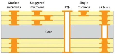
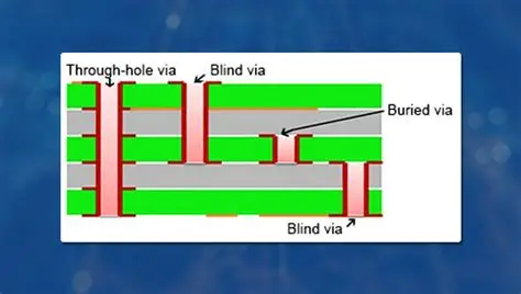
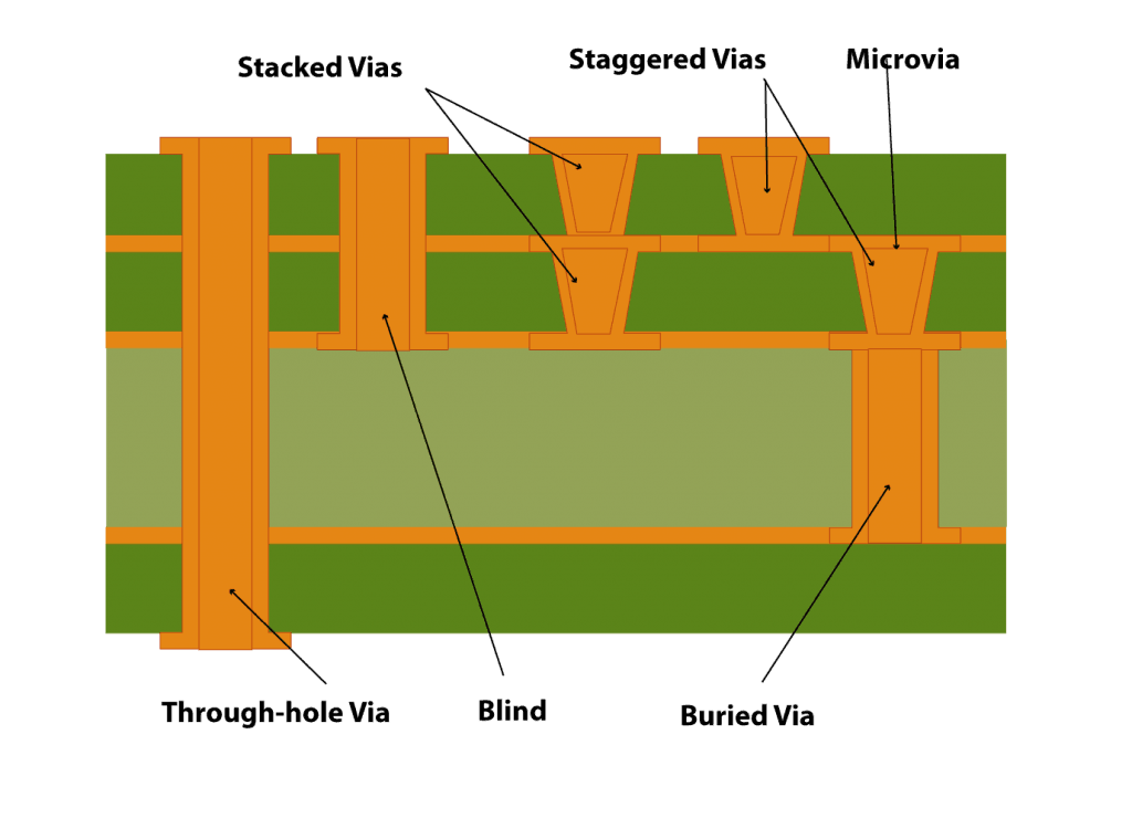
Blind and buried vias enable higher component density and improved signal integrity in multilayer printed circuit boards. These via types connect specific layers without traversing the entire board thickness, unlike conventional through vias. Engineers adopt them when board real estate is limited or when high-speed signals require shorter return paths. The PCB design process benefits from early via planning because it influences layer stackup decisions and routing efficiency. Proper implementation reduces the need for additional layers while maintaining manufacturability.
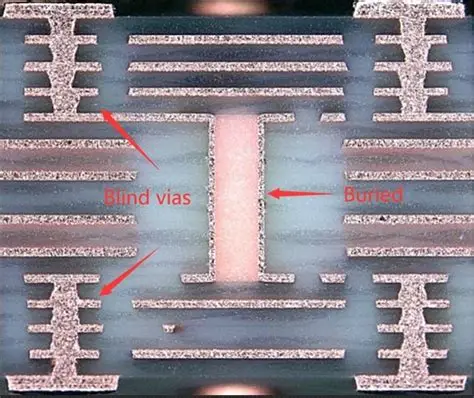
A blind via starts at an outer layer and terminates at one or more inner layers without exiting the opposite side. A buried via connects only internal layers and remains invisible from the board surfaces. Both types support compact layouts in high-density interconnect designs. Their use becomes relevant when through vias would consume excessive routing channels or introduce unwanted inductance. In the PCB design process, these vias help optimize space for fine-pitch components and controlled-impedance traces.
Layer stackup directly affects via feasibility because the chosen dielectric thicknesses and copper weights determine drill depths and aspect ratios. Early consideration of blind and buried vias during stackup definition prevents later redesign cycles. Routing strategy also changes because these vias free up surface and inner-layer real estate for additional traces. Design teams therefore evaluate via types alongside component placement and power distribution requirements.
What Are Blind and Buried Vias and Why They Matter
Technical Principles
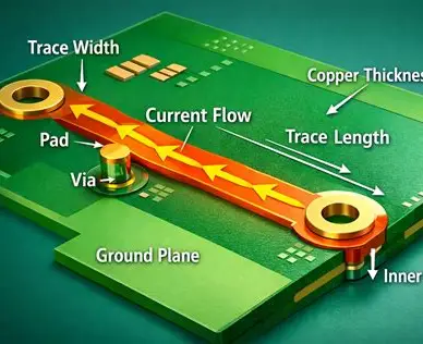
Blind and buried vias rely on controlled-depth drilling or sequential lamination processes during fabrication. The aspect ratio, defined as via depth divided by diameter, must stay within acceptable limits to ensure reliable plating. Signal integrity improves because shorter via stubs reduce reflections at high frequencies. Power integrity also benefits when vias provide low-inductance paths between planes. Thermal management considerations arise when high-current paths use these vias, requiring adequate copper plating thickness.
Layer-to-layer registration tolerances influence via placement rules because misalignment can cause opens or shorts. Design rules therefore incorporate minimum annular ring sizes and clearance requirements specific to each via type. The overall board thickness and number of layers further constrain the maximum number of sequential lamination cycles. These constraints guide the selection between blind, buried, or through vias during the initial planning phase.
Practical Solutions and Best Practices
Begin the PCB design process with via planning that maps every required interconnection to the appropriate via type. Identify signals that can use buried vias to keep outer layers clear for components and test points. Next, finalize the layer stackup with input from fabrication guidelines so that blind via depths align with available dielectric thicknesses. Document the stackup with explicit via start and stop layers for each net class.
During routing, apply a consistent via strategy that minimizes the total number of vias while preserving signal integrity. Place blind vias near component pads when escape routing from fine-pitch devices is required. Route critical high-speed nets with buried vias to shorten stub lengths. Review the entire layout for via density hotspots that could affect yield or thermal performance. Perform a formal design review that checks via aspect ratios, clearance violations, and stackup compliance before releasing files for fabrication.
Conclusion
Implementing blind and buried vias requires coordinated decisions across via planning, layer stackup, routing strategy, and design review. When executed systematically, these via types deliver higher routing density and better electrical performance without increasing board size. Engineers who integrate via considerations early in the PCB design process reduce iterations and improve first-pass success. Consistent application of these practices supports reliable, high-density boards that meet modern electronic product requirements.
FAQs
Q1: What role does via planning play in the overall PCB design process?
A1: Via planning establishes the interconnection strategy before detailed routing begins. It determines which nets use blind vias, buried vias, or through vias based on layer access and electrical requirements. Effective planning aligns with layer stackup choices and prevents routing congestion later in the workflow. It also supports design review by providing clear documentation of via start and stop layers for every net class.
Q2: How does layer stackup influence blind and buried via implementation?
A2: Layer stackup defines the available dielectric thicknesses and copper layers that set the possible depths for blind and buried vias. Proper stackup selection ensures via aspect ratios remain manufacturable while meeting impedance targets. Changes to the stackup after routing starts often require via repositioning and additional design iterations. Early stackup definition therefore streamlines the entire PCB design process.
Q3: Why is routing strategy important when using buried vias?
A3: Routing strategy determines how buried vias connect inner layers without interfering with surface components or outer-layer traces. Strategic placement frees routing channels on outer layers and shortens high-speed paths. A well-planned strategy also balances via density across the board to maintain fabrication yield. It integrates directly with design review checkpoints to verify compliance with clearance and aspect-ratio rules.
Q4: What should a design review check regarding blind and buried vias?
A4: A design review verifies that all blind and buried via locations satisfy minimum annular ring and clearance requirements. It confirms via depths align with the approved layer stackup and that aspect ratios fall within acceptable limits. The review also examines via placement relative to component pads and critical traces to ensure signal integrity and manufacturability. Documentation of via types for each net class supports traceability through the PCB design process.
References
IPC-6012E — Qualification and Performance Specification for Rigid Printed Boards. IPC, 2017
IPC-2221B — Generic Standard on Printed Board Design. IPC, 2012
IPC-A-600K — Acceptability of Printed Boards. IPC, 2020