 ALLPCB


Smart grids rely on advanced electronics to monitor, control, and optimize electricity distribution across generation, transmission, and consumption points. Printed circuit boards serve as the foundational hardware in sensors, communication modules, protection relays, and power converters that enable real-time data exchange and automated responses. Reliability of these PCBs directly affects grid stability, because any malfunction can lead to power interruptions, equipment damage, or safety risks in critical infrastructure. Engineers must therefore prioritize designs that withstand harsh operating conditions over decades of service. This focus ensures consistent performance while meeting the stringent demands of utility environments.
Smart grid systems operate in diverse environments that expose PCBs to temperature fluctuations, humidity, vibration, and electrical stresses not typically encountered in consumer electronics. Long-term reliability prevents cascading failures that could disrupt entire distribution networks. Procurement teams and designers evaluate PCB lifespan early in the project cycle to reduce maintenance costs and downtime. Component selection and manufacturing processes play central roles in achieving the required durability. Without adequate attention to these factors, even well-designed systems may experience premature degradation.
The Importance of PCB Reliability in Smart Grid Applications
Smart grid systems operate in diverse environments that expose PCBs to temperature fluctuations, humidity, vibration, and electrical stresses not typically encountered in consumer electronics. Long-term reliability prevents cascading failures that could disrupt entire distribution networks. Procurement teams and designers evaluate PCB lifespan early in the project cycle to reduce maintenance costs and downtime. Component selection and manufacturing processes play central roles in achieving the required durability. Without adequate attention to these factors, even well-designed systems may experience premature degradation.
Key Challenges and Failure Mechanisms in Smart Grid PCBs
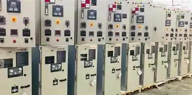
Temperature cycling causes expansion and contraction mismatches between materials, leading to solder joint fatigue and trace cracking over time. Moisture ingress promotes corrosion of copper conductors and electrochemical migration between closely spaced traces. Vibration from transformers or switching equipment accelerates mechanical fatigue in connectors and component leads. High-voltage environments introduce partial discharge and insulation breakdown risks. These mechanisms interact, so a single environmental factor rarely acts in isolation.
Engineers analyze failure modes through systematic approaches that identify root causes before they affect field performance. Thermal gradients across large boards can induce warpage that stresses surface-mount components. Contaminants from manufacturing residues or environmental exposure further lower insulation resistance. Understanding these interactions guides targeted improvements in material choices and layout practices.
Industry Standards Guiding PCB Reliability
Standards from recognized organizations provide frameworks for qualification and performance verification. IPC-6012E outlines qualification and performance requirements for rigid printed boards, helping ensure consistent quality across production lots. Adherence to these guidelines supports traceability and repeatability in manufacturing processes critical for infrastructure applications.
PCB Component Selection for Long Life in Smart Grid Applications
Component selection begins with evaluating operating temperature ranges, voltage ratings, and expected lifetime under combined stresses. High-reliability capacitors and resistors rated for extended temperature operation reduce the likelihood of parametric drift. Connectors with robust contact materials resist oxidation in humid or polluted atmospheres. Designers also consider derating factors that keep components well below maximum specifications to extend overall board life. Material compatibility between the PCB substrate, solder, and components minimizes stress concentrations during thermal excursions.
Accelerated Aging for Smart Grid PCBs
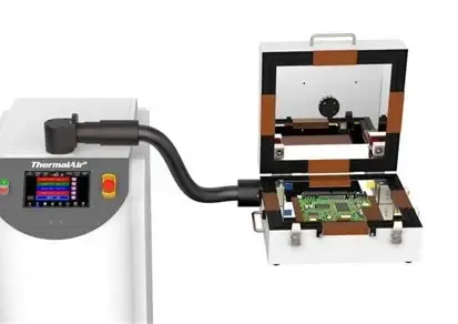
Accelerated aging protocols subject assemblies to elevated temperatures, humidity, and voltage to compress years of service into weeks or months of testing. These methods reveal latent defects such as delamination or via cracking that might otherwise appear only after extended field exposure. Test profiles are developed to correlate with real-world duty cycles while remaining within the capabilities of standard laboratory equipment. Data from these tests informs design iterations and supplier qualification decisions. Consistent application of such methods supports predictive maintenance strategies for utilities.
Failure Analysis of Smart Grid PCBs
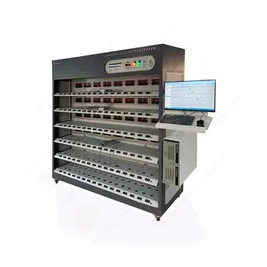
Failure analysis begins with non-destructive techniques such as X-ray imaging and thermal imaging to locate anomalies without damaging the assembly. Subsequent steps may include cross-sectioning to examine internal structures or scanning electron microscopy to characterize fracture surfaces. Root-cause determination distinguishes between design, material, or process-related issues. Documentation of findings feeds back into design rules and supplier audits, closing the loop on continuous improvement. This structured approach minimizes recurrence of similar issues across future projects.
Best Practices for Improving PCB Lifespan in Smart Grid Applications
Conformal coatings provide an additional barrier against moisture and contaminants when applied uniformly and inspected for coverage. Layout practices that incorporate adequate spacing, thermal relief, and strain relief reduce mechanical and electrical stresses. Regular review of material specifications ensures compatibility with evolving environmental requirements. Collaboration between design, manufacturing, and reliability teams identifies potential issues early. These practices collectively contribute to extended service intervals and lower total cost of ownership.
Conclusion
Reliable PCBs form the backbone of smart grid infrastructure, where longevity directly translates to operational continuity and safety. Systematic attention to environmental stresses, component choices, testing protocols, and analysis methods enables engineers to meet demanding performance targets. Integration of established industry practices throughout the product lifecycle supports consistent results across multiple deployments. Continued focus on these areas will remain essential as grids incorporate higher levels of renewable integration and digital control.
FAQs
Q1: What does PCB reliability testing for smart grids typically involve?
A1: PCB reliability testing for smart grids evaluates performance under combined thermal, humidity, and electrical stresses that mirror field conditions. Protocols often include thermal cycling, damp heat exposure, and vibration sequences to identify weaknesses before deployment. Results guide material and design refinements that extend service life in utility environments.
Q2: How is accelerated aging for smart grid PCBs performed?
A2: Accelerated aging for smart grid PCBs uses elevated temperature, humidity, and bias conditions to simulate extended operational periods in compressed timeframes. Engineers correlate test duration and severity with expected field lifetimes using established models. This approach reveals potential failure modes early and supports qualification of new designs or suppliers.
Q3: Why is failure analysis of smart grid PCBs important?
A3: Failure analysis of smart grid PCBs identifies root causes of malfunctions through systematic inspection and characterization techniques. Findings inform corrective actions in design, materials, or processes that prevent recurrence. Thorough analysis supports continuous improvement and maintains high availability in critical power infrastructure.
Q4: What factors influence PCB component selection for long life in smart grids?
A4: PCB component selection for long life in smart grids considers temperature ratings, voltage derating, material compatibility, and resistance to environmental degradation. Engineers evaluate supplier data and perform additional qualification testing to confirm suitability. Proper selection reduces parametric drift and mechanical failures over decades of service.
References
[IPC-6012E — Qualification and Performance Specification for Rigid Printed Boards. IPC, 2017]
[JEDEC J-STD-020E — Moisture/Reflow Sensitivity Classification. JEDEC, 2014]
[IEC 60068-2-14 — Environmental Testing — Part 2-14: Tests — Test N: Change of Temperature. IEC, 2009]





