 ALLPCB


In high-speed PCB design, engineers must balance increasing component density with reliable signal transmission. Stacked vias provide vertical interconnects across multiple layers while supporting finer pitch layouts. These structures help route signals in complex boards without excessive horizontal space. However, their geometry directly influences impedance characteristics. Proper management of stacked via impedance control ensures consistent performance across high-frequency applications. Designers therefore evaluate via configurations early in the layout process to meet overall system requirements.
What Are Stacked Vias and Why Impedance Control Matters
Stacked vias consist of multiple via segments aligned vertically and connected end to end through intermediate pads. This construction differs from single through-hole vias or staggered arrangements by allowing direct layer-to-layer transitions without lateral offsets. In high-speed PCB design, such vias support the miniaturization needed for advanced electronics. Impedance control becomes essential because any deviation causes signal reflections that degrade performance. Controlled impedance vias maintain the target characteristic impedance along the entire path, preserving signal integrity. Without this control, reflections increase bit error rates and limit operating frequencies.
Technical Principles of Stacked Via Impedance Behavior
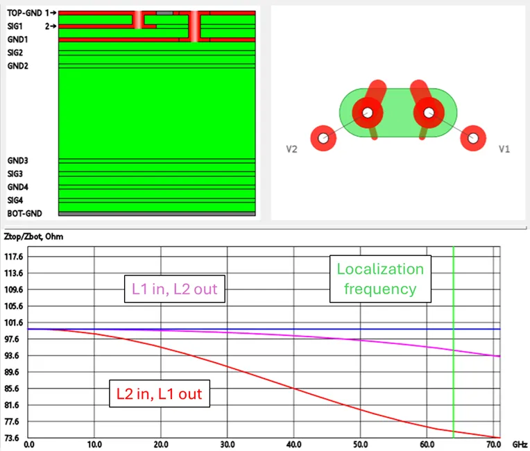
The impedance of a via depends on its diameter, pad size, anti-pad clearance, and the surrounding dielectric materials. Stacked vias add complexity because each segment contributes parasitic capacitance and inductance. These parasitics arise from the barrel plating, the pad overhang, and the proximity to reference planes. In high-frequency operation, the via acts as a short transmission line segment whose impedance must match the connected traces. Mismatches occur when via geometry alters the effective inductance or capacitance relative to the board stack-up. Engineers therefore calculate via impedance using electromagnetic field solvers that account for the full three-dimensional structure. Accurate modeling reveals how changes in drill size or pad diameter shift the impedance profile.
Signal integrity suffers when via stubs or abrupt transitions excite higher-order modes. Stacked configurations can shorten stubs compared with through vias, yet residual discontinuities still require compensation. Dielectric constant variations between layers further influence the local impedance. Consistent material properties across the stack-up help stabilize performance. Thermal expansion differences during manufacturing may also alter via geometry slightly, affecting final impedance values.
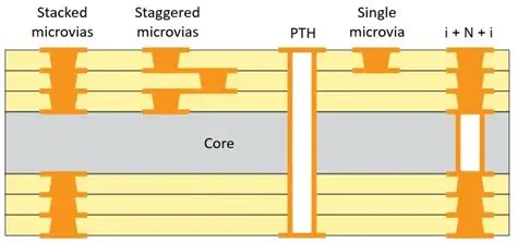
Best Practices for Controlled Impedance Vias in High-Speed Designs
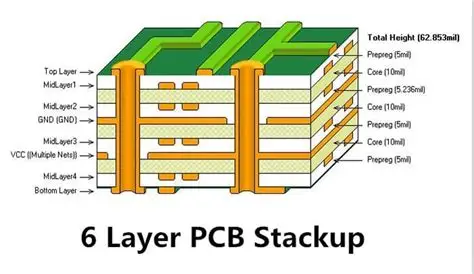
Designers begin by defining target impedance values based on trace geometry and stack-up parameters. Via dimensions are then selected to achieve a matching impedance, often verified through simulation before layout finalization. Pad sizes are minimized while maintaining sufficient annular ring for reliability. Anti-pad clearances are optimized to reduce excess capacitance. Layer transitions are planned to keep reference planes continuous near the via.
Back-drilling or blind and buried via combinations serve as alternatives when full stacks introduce excessive inductance. Material selection follows IPC standards to ensure dielectric consistency. IPC-2221 provides foundational guidance on printed board design parameters that influence via performance. Simulation tools model the via as part of the transmission path, allowing iterative adjustments. Fabrication tolerances are communicated clearly so that actual boards meet the simulated impedance targets.
Challenges and Mitigation Strategies
Manufacturing variations in plating thickness or drill registration can shift via impedance outside acceptable limits. Engineers address this by specifying tighter tolerances on critical dimensions and requesting test coupons for impedance verification. Thermal cycling may induce micro-cracks that alter electrical performance over time. Selecting appropriate copper weights and via fill materials improves mechanical stability. In dense layouts, via-to-via coupling introduces additional crosstalk that must be modeled alongside impedance.
Testing at the board level confirms that fabricated vias meet design goals. Time-domain reflectometry measurements identify impedance discontinuities along signal paths. When deviations appear, designers review stack-up symmetry and via aspect ratios. Adjustments in subsequent revisions focus on balancing density requirements with electrical performance.
Conclusion
Stacked vias enable the compact routing demanded by modern high-speed electronics, yet they require deliberate impedance engineering. Understanding the parasitic effects of via geometry and maintaining consistent stack-up parameters supports reliable signal integrity. Simulation combined with adherence to established design guidelines reduces the risk of reflections and performance degradation. Practical attention to tolerances and verification steps ensures that controlled impedance vias perform as intended across production volumes. These considerations help engineers deliver robust boards that meet both density and electrical requirements.
FAQs
Q1: How do stacked vias affect impedance matching in high-speed PCB design?
A1: Stacked vias introduce parasitic inductance and capacitance that can deviate from the target impedance of connected traces. Proper dimensioning and simulation allow designers to match via impedance to the surrounding transmission lines. This matching preserves signal integrity by minimizing reflections at layer transitions. Consistent dielectric properties and optimized pad geometries further support accurate impedance control throughout the path.
Q2: What role does via geometry play in controlled impedance vias?
A2: Via diameter, pad size, and anti-pad clearance directly determine the capacitance and inductance that set the via impedance. In stacked configurations, each segment adds to the overall electrical length and must be modeled together. Adjusting these parameters during design brings the via impedance into alignment with trace requirements. Accurate control of these dimensions supports predictable high-frequency behavior.
Q3: Why is signal integrity critical when using stacked vias?
A3: Signal integrity depends on maintaining uniform impedance to prevent reflections that distort waveforms. Stacked vias can create discontinuities if their impedance differs from adjacent traces. Careful design and verification ensure that high-speed signals propagate without excessive loss or timing errors. This consistency is essential for reliable operation in demanding applications.
Q4: How can engineers verify impedance control after fabrication?
A4: Test coupons incorporated into the panel allow measurement of via impedance using time-domain reflectometry. Results are compared against design targets to confirm that manufacturing tolerances have been met. Any deviations prompt review of stack-up or via parameters for future builds. This verification step confirms that controlled impedance vias perform as simulated.
References
IPC-2221B - Generic Standard on Printed Board Design. IPC, 2012
IPC-6012E - Qualification and Performance Specification for Rigid Printed Boards. IPC, 2017
IPC-A-600K - Acceptability of Printed Boards. IPC, 2020





