ALLPCB


Prototyping and Testing Robotics Control PCBs: Ensuring Functionality and Performance
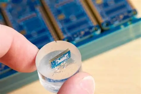
Robotics control systems rely on printed circuit boards to manage motors, sensors, and communication interfaces with precision. These boards must handle continuous operation under mechanical stress, temperature fluctuations, and electromagnetic interference. Prototyping allows engineers to validate designs before full production, while systematic testing confirms that each unit meets performance requirements. Effective processes reduce the risk of field failures and support consistent operation in demanding environments.
Why Prototyping and Testing Matter for Robotics Applications
Robotics platforms operate in dynamic conditions that place unique demands on control electronics. Vibration from movement, rapid thermal cycling, and exposure to dust or moisture can degrade board performance over time. Thorough prototyping identifies layout or component issues early, while comprehensive testing verifies electrical integrity and long-term reliability. This approach supports safe and predictable robot behavior across industrial, collaborative, and mobile applications.
Core PCB Testing Methods Used in Robotics Development
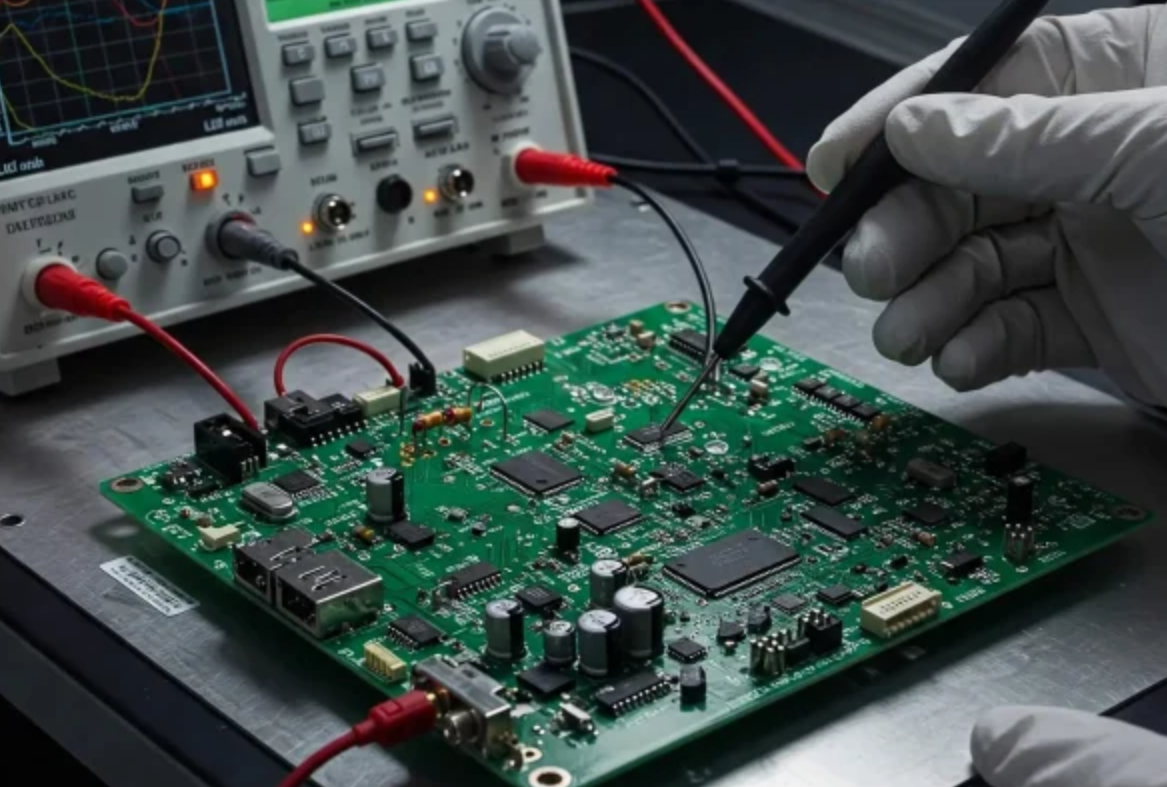
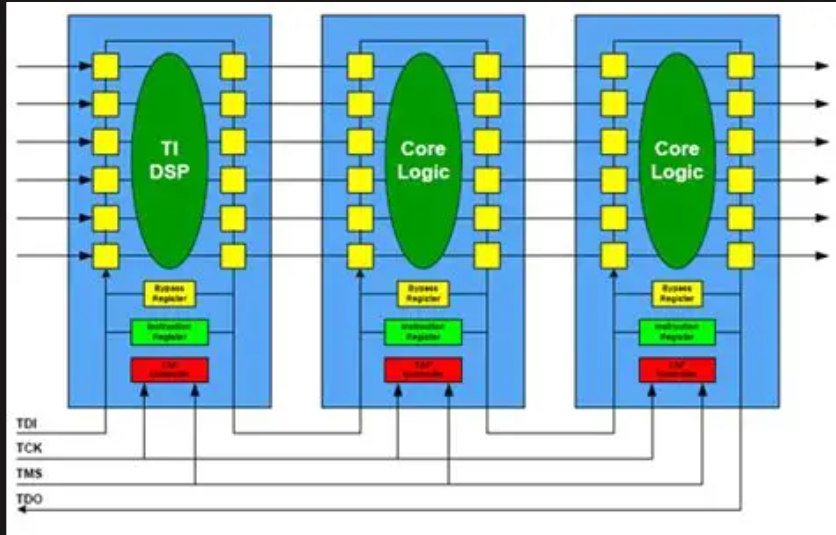
Several established testing approaches evaluate robotics control boards at different stages. In-circuit testing applies probes to verify component values, opens, and shorts on assembled boards. Functional testing exercises the complete circuit under simulated operating conditions to confirm logic, signal integrity, and power delivery. Boundary scan testing uses built-in test access ports to check interconnects and device functionality without physical probing of every node. These methods complement one another and provide layered confidence in board quality.
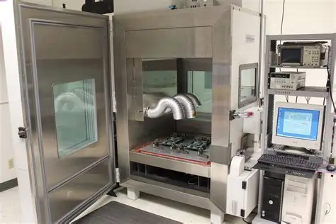
Environmental testing subjects prototypes to controlled stress conditions that replicate real-world use. Temperature cycling, humidity exposure, and vibration sequences reveal weaknesses in solder joints, materials, or layout. Highly accelerated life testing (HALT) and highly accelerated stress screening (HASS) apply extreme conditions to uncover design margins and screen production units efficiently. Such protocols help ensure that robotics PCBs maintain performance when deployed in variable industrial or outdoor settings.
Design Considerations and Best Practices for Prototyping
Successful robotics PCB prototyping begins with design choices that facilitate both manufacturing and testing. Test points should be placed accessibly, and boundary scan chains should be implemented where component complexity warrants it. Material selection follows performance specifications outlined in IPC-6012E for rigid printed boards, ensuring adequate thermal and mechanical properties. Careful attention to trace routing, ground planes, and decoupling reduces noise and supports stable operation of high-speed control signals.
Assembly processes must align with quality criteria defined in IPC-A-600K to minimize defects that could affect reliability. Moisture sensitivity of components is managed according to JEDEC J-STD-020E guidelines during storage and reflow. Iterative prototype builds allow engineers to refine layouts based on measured performance data rather than assumptions. Documentation of each revision supports traceability and accelerates troubleshooting when issues arise.
Reliability Validation Through Environmental and Accelerated Testing
Environmental and accelerated testing provide data on how robotics control boards behave under sustained stress. HALT identifies operating limits by progressively increasing temperature, vibration, and other stressors until failure occurs. HASS then applies tailored stress profiles to production samples to precipitate latent defects before shipment. These techniques complement standard environmental sequences and help establish confidence intervals for expected service life.
Thermal imaging and warpage measurement during testing reveal mechanical distortions that could compromise connections over time. Consistent application of these methods across prototype and production phases supports repeatable quality outcomes. Engineers review test results against predefined acceptance criteria to decide whether a design iteration is required.
Conclusion
Prototyping combined with structured testing forms the foundation for reliable robotics control PCBs. Methods such as in-circuit testing, functional verification, boundary scan, and environmental stress screening address electrical, mechanical, and environmental risks systematically. Adherence to recognized industry standards guides material and process decisions without introducing unnecessary complexity. The result is control electronics that perform consistently in the varied conditions typical of robotic systems.
FAQs
Q1: What distinguishes robotics PCB prototyping from standard board development?
A1: Robotics PCB prototyping emphasizes validation under mechanical vibration, thermal cycling, and electromagnetic conditions typical of motion systems. Engineers use iterative builds to confirm signal integrity and power stability before committing to volume production. This focused approach reduces the likelihood of performance issues once boards are integrated into complete robots.
Q2: Which PCB testing methods are most effective for robotics control boards?
A2: In-circuit testing, functional testing, and boundary scan testing together provide comprehensive coverage of component-level and system-level behavior. Environmental testing and HALT/HASS further evaluate long-term durability under stress. Selecting the right combination depends on board complexity and the specific operating environment of the robot.
Q3: How does environmental testing improve robotics PCB reliability?
A3: Environmental testing exposes prototypes to temperature extremes, humidity, and vibration that mirror actual deployment conditions. Accelerated methods such as HALT/HASS reveal design margins and screen for latent defects. The data obtained guides refinements that help boards maintain functionality throughout their intended service life.
Q4: Why is design for testability important in robotics PCB projects?
A4: Design for testability incorporates accessible test points, boundary scan architecture, and clear signal paths that simplify verification. These features reduce test time and improve fault coverage during both prototyping and production. The result is faster iteration cycles and higher confidence in final board performance.
References
IPC-6012E — Qualification and Performance Specification for Rigid Printed Boards. IPC, 2017
IPC-A-600K — Acceptability of Printed Boards. IPC, 2020
JEDEC J-STD-020E — Moisture/Reflow Sensitivity Classification. JEDEC, 2014