ALLPCB


Introduction
Smart grids rely on advanced power conversion systems to manage electricity flow from generation sources to end users with minimal losses. Printed circuit boards serve as the foundation for these converters, handling high currents and voltages while maintaining signal integrity. Effective PCB design directly influences overall system efficiency, reliability, and compliance with operational demands in modern energy networks. Engineers focus on layout techniques that support bidirectional power flow and integration with renewable sources. This approach ensures stable performance across varying load conditions typical in smart grid environments.
Why PCB Design Matters for Power Converters in Smart Grids
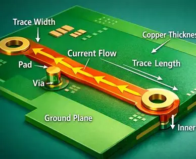
Power converters in smart grids perform essential functions such as voltage regulation, frequency conversion, and energy storage interfacing. The PCB acts as the structural and electrical backbone that connects semiconductors, inductors, capacitors, and control circuits. Poor layout choices can lead to increased resistance paths, excessive heat buildup, and unwanted electromagnetic interference that disrupts grid stability. High-current PCB layout for smart grid applications requires careful trace sizing and layer stacking to handle loads often exceeding tens of amperes without voltage drops. These design decisions contribute to reduced operational costs and extended equipment lifespan in utility-scale deployments. Proper planning at the board level supports the scalability needed for expanding smart grid infrastructure.
Technical Principles Behind Efficient Energy Conversion on PCBs
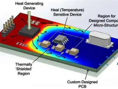
Power efficiency in smart grid PCB design begins with minimizing conduction and switching losses through optimized copper distribution and component placement. High-current paths demand wider traces or multiple parallel layers to lower resistance and prevent localized heating. Thermal management for power electronics involves strategic use of thermal vias, heat sinks, and copper pours that transfer heat away from active devices toward board edges or mounting points. Electromagnetic interference arises from rapid current changes in switching circuits, creating radiated and conducted noise that can affect nearby control signals. Minimizing EMI in smart grid power PCBs requires separation of power and signal planes, along with shielding techniques and filtered return paths. These principles work together to maintain conversion efficiencies above typical thresholds while preserving electromagnetic compatibility in dense installations.
Practical Solutions for High-Current PCB Layout in Smart Grid Applications
Engineers begin layout by identifying primary current paths and assigning dedicated layers or thick copper weights to those routes. Component orientation plays a key role, with power devices positioned to shorten high-current loops and reduce parasitic inductance. Ground planes should remain continuous beneath switching elements to provide low-impedance return paths and contain magnetic fields. Thermal relief patterns around high-power pads balance mechanical strength with heat dissipation needs during assembly and operation. Simulation tools help validate voltage drop and temperature rise before fabrication, allowing iterative refinements. These steps collectively improve power efficiency in smart grid PCB design by addressing both electrical and thermal constraints in a single integrated approach.
Addressing EMI and Thermal Challenges in Power Electronics Boards
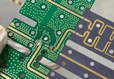
Effective EMI control starts with frequency-aware partitioning that isolates noisy power stages from sensitive analog or digital sections. Differential pair routing for control signals and proper decoupling capacitor placement near integrated circuits suppress high-frequency noise. For thermal performance, designers incorporate embedded heat spreaders or select substrates with enhanced thermal conductivity to manage heat from dense power modules. Ventilation slots or edge-mounted heat sinks further aid airflow in enclosed grid equipment. Compliance with established practices ensures boards withstand continuous operation under elevated ambient temperatures common in substation environments. Combining these measures reduces failure rates and supports long-term grid reliability without excessive redesign cycles.
Improving Overall System Performance Through Integrated Design Choices
Layer stackup selection influences both impedance control and heat spreading, with four or six layer constructions often providing balanced performance for mixed-signal power boards. Material selection focuses on dielectric properties that maintain stability across temperature swings while supporting high voltage isolation. Trace geometry optimization, including rounded corners and tapered transitions, minimizes stress concentrations and improves current carrying capacity. Regular design reviews incorporate feedback from thermal imaging and power loss measurements to refine subsequent iterations. These integrated choices deliver measurable gains in conversion efficiency and electromagnetic compatibility for smart grid deployments.
Conclusion
PCB design forms a critical link in achieving efficient energy conversion within smart grid systems. Attention to high-current paths, thermal pathways, and EMI containment yields boards that operate reliably under demanding conditions. Structured application of layout principles supports both immediate performance targets and future scalability requirements. Continued focus on these elements helps engineers meet evolving grid demands with robust, efficient hardware solutions.
FAQs
Q1: How does PCB design for power converters in smart grids affect overall energy efficiency?
A1: PCB design for power converters in smart grids influences efficiency through reduced resistive losses, optimized thermal paths, and controlled electromagnetic behavior. Engineers size traces and select layer configurations to handle high currents while limiting voltage drops. Thermal management features prevent overheating that would otherwise increase losses or trigger protective shutdowns. Careful component placement and plane design further support stable operation across load variations typical in grid applications. These factors combine to maintain high conversion performance over extended service periods.
Q2: What considerations guide high-current PCB layout for smart grid applications?
A2: High-current PCB layout for smart grid applications prioritizes low-resistance paths using wide traces, parallel layers, or heavy copper weights. Placement of power semiconductors minimizes loop areas to reduce inductance and associated voltage spikes. Thermal vias and copper pours direct heat away from critical components toward dissipation areas. Ground continuity beneath high-current sections provides effective return paths and contains fields. Validation through simulation confirms performance before committing to fabrication.
Q3: Why is minimizing EMI in smart grid power PCBs important for system reliability?
A3: Minimizing EMI in smart grid power PCBs prevents interference with control circuits and communication links essential for grid coordination. Rapid switching generates noise that can couple into adjacent traces or radiate externally, affecting measurement accuracy and protection functions. Techniques such as plane separation, filtering, and shielding contain emissions within acceptable limits. This containment supports uninterrupted operation and compliance with electromagnetic compatibility expectations in utility environments. Proper implementation reduces troubleshooting time during commissioning and maintenance.
Q4: How does PCB thermal management for power electronics improve long-term performance?
A4: PCB thermal management for power electronics directs heat away from semiconductors and passive components through vias, pours, and material choices. Elevated temperatures accelerate aging of solder joints and dielectrics, leading to earlier failures in continuous-duty grid equipment. Effective heat spreading maintains devices within rated operating ranges, preserving efficiency and preventing derating. Integration of these features during layout supports consistent performance across seasonal temperature extremes encountered in field installations.
References
IPC-6012E — Qualification and Performance Specification for Rigid Printed Boards. IPC, 2017
J-STD-001H — Requirements for Soldered Electrical and Electronic Assemblies. IPC, 2020
ISO 9001:2015 — Quality Management Systems. ISO, 2015