 ALLPCB


Introduction
Deciding between small PCB batch production and large PCB batch production often determines the success of electronics projects for electrical engineers. Small-scale runs suit early-stage development where flexibility trumps volume, while large-scale efforts optimize for efficiency in mature designs. This article delivers a thorough PCB production volume analysis to guide scaling PCB manufacturing decisions. Engineers must weigh factors like cost structures, lead times, and quality assurance to align production with project timelines and budgets. Factory processes reveal distinct workflows for each approach, ensuring reliability across volumes. Understanding these differences empowers informed choices without unnecessary expenses or delays.
Defining Small-Scale PCB Batch Production
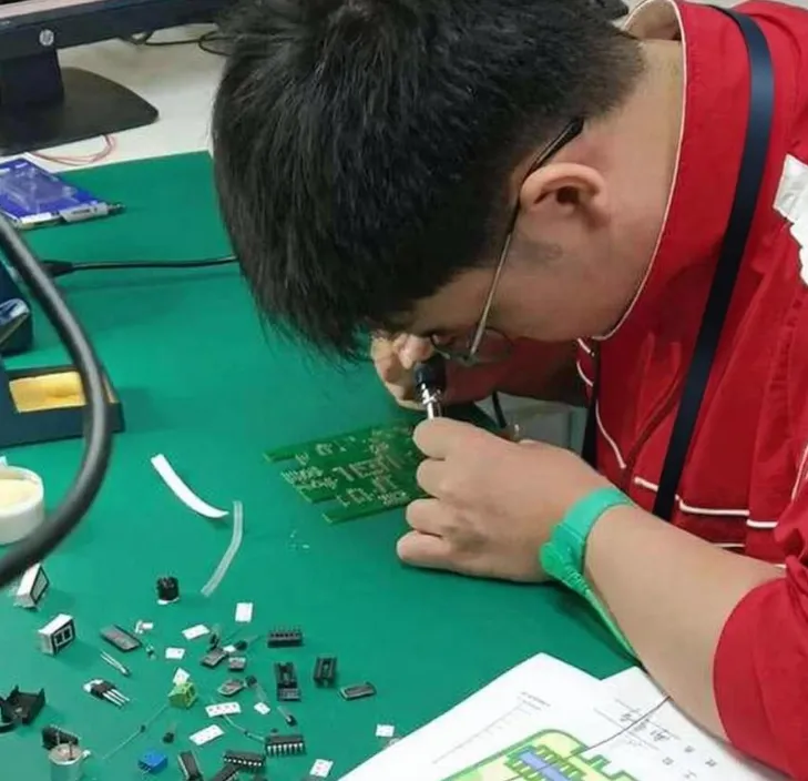
Small PCB batch production typically involves quantities from a single prototype up to a few hundred boards. This approach excels in research and development phases, allowing rapid iterations based on testing feedback. Factories prioritize quick setup times, often using standard panel sizes to minimize tooling costs. Engineers benefit from shorter lead times, sometimes as fast as days, which supports agile design cycles. However, per-unit costs remain higher due to fixed setup expenses spread over fewer pieces. Quality checks focus on individual board verification to catch defects early in low-volume runs.
Defining Large-Scale PCB Batch Production
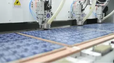
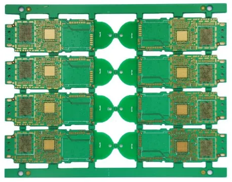
Large PCB batch production handles thousands or tens of thousands of boards, geared toward commercial deployment. Economies of scale drive down per-unit costs through optimized material utilization and automated processes. Factories invest in dedicated tooling, such as custom panels and stencils, to streamline high-volume fabrication. Lead times extend to weeks or months, reflecting the complexity of supply chain coordination and extended testing. This method demands design stability, as changes mid-run incur significant rework expenses. Production emphasizes throughput, with inline inspections maintaining consistency across massive quantities.
Key Differences in PCB Production Volume Analysis
Cost structures diverge sharply between small and large PCB batch production. In small-scale, setup fees dominate, including imaging and etching preparations that do not scale down efficiently. Large-scale amortizes these over vast quantities, slashing material and labor costs per board. Engineers conducting PCB production volume analysis must model total cost of ownership, factoring in inventory holding and potential scrap rates.
Lead times reflect process maturity levels. Small batches leverage flexible scheduling in factories, enabling same-week delivery for urgent prototypes. Large runs require procurement of bulk materials and progressive quality gates, extending timelines but ensuring supply reliability.
Quality control adapts to volume demands. Small-scale often employs 100% visual and electrical testing per board, aligning with IPC-A-600K acceptability criteria for printed boards. Large-scale shifts to statistical process control, sampling batches to verify compliance without halting lines.
Tooling and material choices further differentiate approaches. Small batches use generic panels, reducing upfront investment but limiting customization. Large-scale customizes fixtures for precision, enhancing yield in multilayer boards.
Technical Principles Behind Batch Size Choices
The engineering mechanisms of PCB fabrication highlight why volume affects outcomes. In small PCB batch production, photolithography and plating steps run on smaller panels, increasing edge waste and setup recalibrations. This leads to variable yields, typically managed through overproduction buffers. Electrical engineers analyze trace impedance and via reliability under IPC-6012E specifications for rigid printed boards, ensuring prototypes mirror final performance.
Scaling PCB manufacturing introduces thermal management challenges in large batches. Uniform heating in ovens becomes critical to prevent warpage, addressed via controlled ramp rates per JEDEC J-STD-020E for moisture sensitivity. Factories monitor panel flatness post-lamination, as higher volumes amplify material inconsistencies.
Multilayer builds complicate both scales differently. Small runs tolerate minor registration errors via manual adjustments, while large-scale demands automated optical alignment for sub-mil tolerances. Solder mask application shifts from flood-and-etch in low volume to direct imaging in high volume, improving edge definition.
Yield optimization follows statistical models. Small batches achieve 90-95% yields through individualized handling, whereas large-scale targets 98%+ via process capability indices (Cpk) exceeding 1.33. Engineers use failure mode analysis to predict volume impacts on reliability.
Factors to Consider for Your Project
Project stage dictates batch strategy in PCB production volume analysis. Prototyping favors small PCB batch production for cost-effective validation of signal integrity and power distribution. Production ramps benefit from large-scale once designs pass environmental stress screening.
Budget constraints interplay with volume. Small runs suit constrained funds, avoiding large tooling outlays. Large-scale unlocks savings only with predictable demand, as excess inventory ties up capital.
Design maturity influences scalability. Frequent revisions post-gerber release favor small batches to incorporate fixes swiftly. Stable layouts with verified stackups enable large PCB batch production confidently.
Market dynamics and regulatory needs add layers. Short product lifecycles demand small-scale flexibility, while long-term deployments like industrial controls justify large volumes. Compliance to ISO 9001:2015 quality systems ensures traceability across scales.
Supply chain resilience matters too. Small batches source from multiple vendors for redundancy, mitigating delays. Large-scale secures dedicated suppliers for consistent laminate grades.
Best Practices for Small PCB Batch Production
Optimize panelization to maximize board count per panel without compromising spacing. Engineers specify v-scoring or tab-routing suited to low-volume handling. Select standard copper weights and finishes like HASL or ENIG for broad compatibility.
Prioritize design-for-manufacturability (DFM) reviews early. Avoid blind vias or fine-pitch components unless tested, as small runs limit yield recovery. Request electrical test fixtures only for critical nets to control costs.
Collaborate with factories on material choices. FR-4 grades suffice for most prototypes, but specify Tg values matching end-use temperatures. Implement bake-out processes per JEDEC guidelines to prevent popcorn effects during assembly.
Document iterations rigorously. Maintain revision histories in gerbers and BOMs to track changes. Use flying probe testing for comprehensive opens/shorts checks without dedicated bed-of-nails.
Best Practices for Large PCB Batch Production
Invest in upfront DFM and DFA analysis to lock in stable designs. Simulate warpage and CTE mismatch using factory-provided models. Standardize layer counts and via types to leverage existing tooling libraries.
Qualify processes via first-article inspections under IPC-6012E. Establish golden samples for ongoing comparisons. Transition to automated optical inspection (AOI) and X-ray for inner layers.
Bulk procurement stabilizes costs but requires storage protocols. Segregate lots by IPC class to prevent cross-contamination. Forecast volumes with buffers for yield losses in high-density interconnects (HDI).
Monitor ongoing metrics like first-pass yield and escape rates. Adjust etch factors and plating chemistry iteratively. Scale testing to AQL sampling plans aligned with end-customer expectations.
Real-World Insights from Factory Floors
Consider a sensor module transitioning from prototype to deployment. Initial small PCB batch production of 50 units validated firmware integration and EMI compliance swiftly. Scaling to 5,000 pieces required panel redesign and stencil optimization, reducing defects by refining solder paste volume.
In power electronics, large batches exposed thermal vias inconsistencies missed in small runs. Factory adjustments per IPC standards improved heat dissipation uniformity. Such insights underscore volume-specific debugging.
Engineers scaling PCB manufacturing often hybridize approaches. Pilot large-batch runs at reduced scale to de-risk full production. This balances cost with validation.
Conclusion
Small PCB batch production offers agility for development, while large PCB batch production delivers efficiency for volume needs. PCB production volume analysis reveals trade-offs in cost, time, and quality that guide scaling PCB manufacturing. Electrical engineers succeed by matching batch size to project maturity, budget, and demand forecasts. Adhering to standards like IPC and JEDEC ensures reliability across scales. Evaluate your requirements holistically to select the right path, optimizing both innovation and profitability.
FAQs
Q1: What is small PCB batch production, and when should electrical engineers choose it?
A1: Small PCB batch production covers low volumes like 1 to 500 boards, ideal for prototypes and custom designs. Engineers opt for it during R&D to enable quick iterations and testing without high tooling costs. Factories provide fast lead times, supporting agile workflows. This approach minimizes financial risk for unproven concepts while maintaining quality per IPC guidelines.
Q2: How does large PCB batch production differ in cost from small-scale?
A2: Large PCB batch production lowers per-unit costs through economies of scale, amortizing setups over thousands of boards. Small-scale incurs higher relative setup and material expenses. Engineers perform PCB production volume analysis to breakeven points, typically above 1,000 units. Factory processes like automated lines further reduce labor in high volumes.
Q3: What factors influence scaling PCB manufacturing decisions?
A3: Key factors include design stability, demand forecasts, and budget. Early-stage projects favor small batches for flexibility, while mature products suit large-scale efficiency. Lead times, quality controls, and material availability also weigh in. Standards like ISO 9001 ensure scalable processes across transitions.
Q4: Can small PCB batch production meet the same quality as large-scale?
A4: Yes, with rigorous per-board inspections aligned to IPC-A-600K. Small runs use 100% testing to match large-scale statistical controls. Engineers verify compliance through DFM and prototypes. Volume does not compromise standards if processes adapt appropriately.
References
IPC-6012E — Qualification and Performance Specification for Rigid Printed Boards. IPC, 2017
IPC-A-600K — Acceptability of Printed Boards. IPC, 2020
JEDEC J-STD-020E — Moisture/Reflow Sensitivity Classification. JEDEC, 2014
ISO 9001:2015 — Quality Management Systems. ISO, 2015


