ALLPCB


Introduction
PTFE PCBs, prized for their low dielectric constant and minimal signal loss in high-frequency applications, present unique hurdles during assembly. Electric engineers often encounter issues with component placement and soldering due to the material's mechanical properties, such as low modulus of elasticity and coefficient of thermal expansion (CTE) mismatch with metals. These challenges can lead to defects like warpage, poor solder wetting, and joint reliability failures if not addressed properly. This article explores practical troubleshooting strategies for PTFE PCB surface mount assembly, PTFE PCB reflow soldering, and PTFE PCB wave soldering, drawing on established engineering principles. By understanding these pain points, teams can optimize processes to achieve robust assemblies suitable for demanding RF and microwave environments.
Understanding PTFE PCBs and Assembly Demands
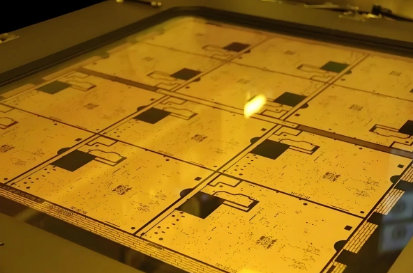
PTFE, or polytetrafluoroethylene, serves as a core substrate in PCBs for applications requiring superior electrical performance, including radar systems and telecommunications. Unlike standard FR-4, PTFE exhibits a softer texture and greater susceptibility to deformation under mechanical stress, complicating precision tasks like component pick-and-place. Its CTE closely matches copper in the plane but diverges in the Z-axis, exacerbating warpage during thermal cycling in assembly. These traits make PTFE PCB assembly a troubleshooting focal point, where even minor process deviations can compromise signal integrity. Engineers must prioritize material-specific handling to maintain coplanarity and alignment throughout surface mount and soldering stages.
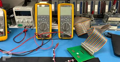
The relevance intensifies in high-volume production, where yield losses from placement errors or solder defects inflate costs. Troubleshooting begins with recognizing how PTFE's low rigidity affects fiducial recognition and nozzle suction during automated placement. Without tailored fixtures or vacuum adjustments, components may shift, leading to open joints or bridges post-reflow. Adhering to standards like IPC J-STD-001 ensures consistent solder joint criteria, guiding process validation.
Key Challenges in Component Placement for PTFE PCBs
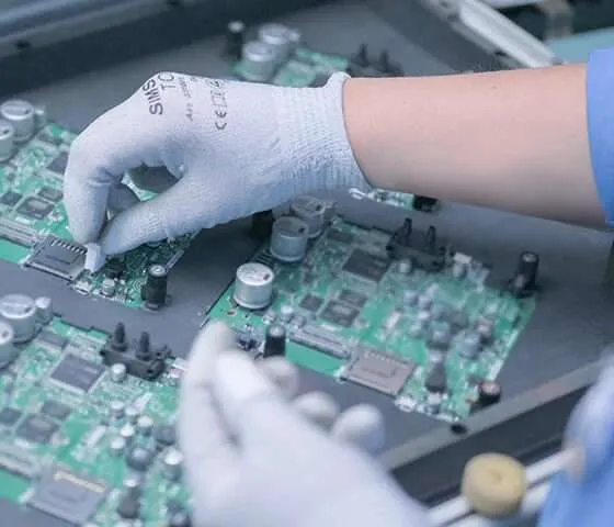
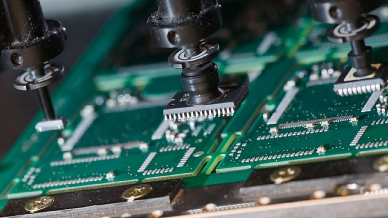
Component placement on PTFE PCBs demands heightened precision because the substrate deforms easily under pick-and-place pressure. Vacuum nozzles can dimple the soft surface, misaligning fiducials and causing offsets in surface mount devices (SMDs). Warpage, often from uneven copper distribution or prior lamination stresses, further disrupts planarity, making it tough for vision systems to lock onto pads. Engineers troubleshooting this report frequent head-in-pillow defects downstream, where components float during reflow due to initial misalignment.
Handling thin PTFE laminates risks cracking or delamination if gripped improperly, especially in high-speed lines. The material's low thermal conductivity also means localized heating from friction can induce micro-warps mid-process. To mitigate, teams implement low-force placement parameters and custom soft-touch end effectors. Visual inspection post-placement reveals subtle shifts invisible to automation, underscoring manual verification's role in PTFE PCB surface mount assembly.
Another hurdle involves adhesive stencils for fine-pitch parts, where PTFE's surface energy resists paste adhesion, leading to insufficient volume. This compounds placement accuracy needs, as under-dosed paste fails to self-align components during reflow. Troubleshooting logs highlight how humidity exacerbates these issues by softening PTFE further. Process controls, like enclosed dry environments, prove essential for repeatable outcomes.
Related Reading: PTFE PCB Materials: Understanding Dielectric Constant and Loss Tangent
Soldering Challenges: Reflow and Wave Processes
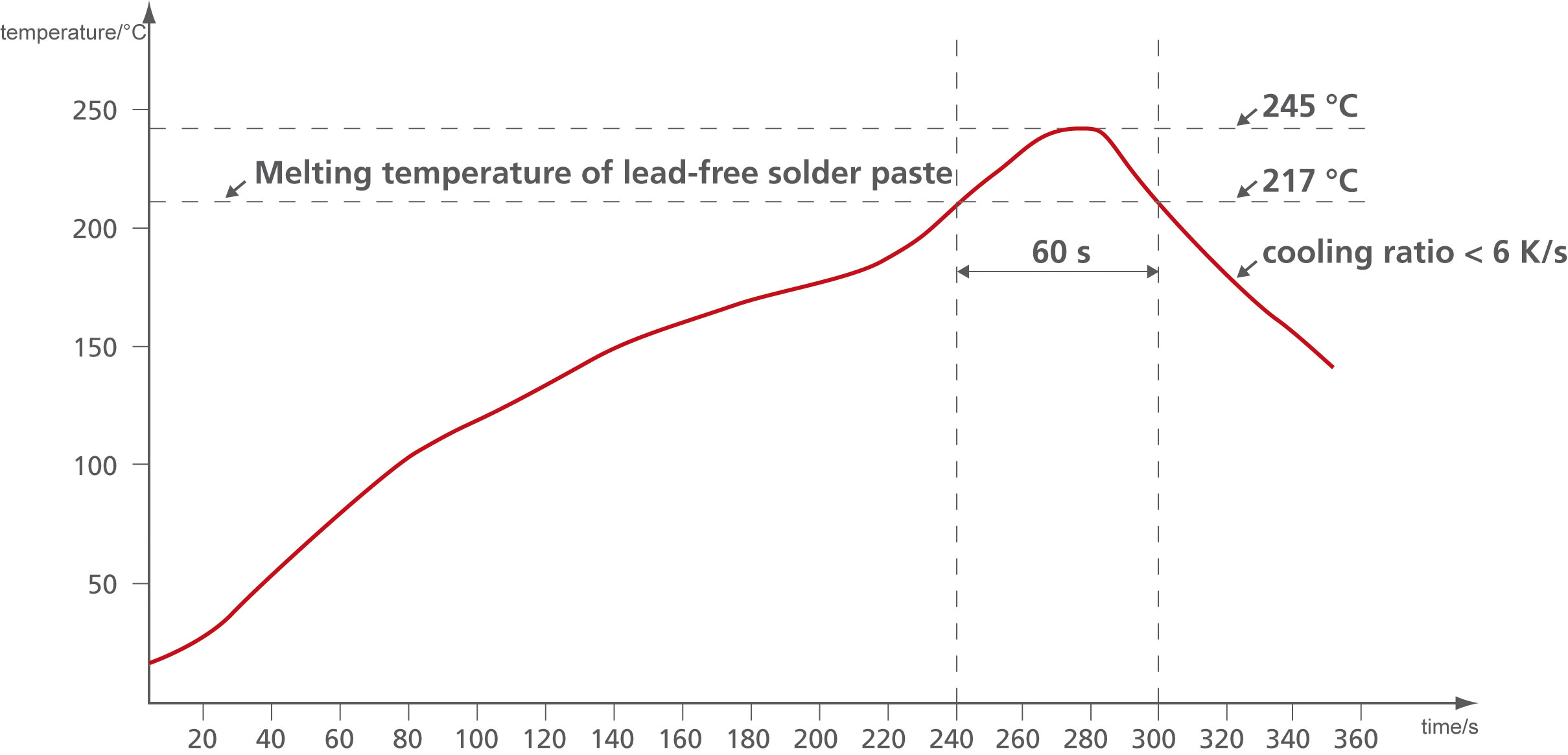
PTFE PCB reflow soldering grapples with thermal mismatch, where rapid heating causes substrate expansion mismatched to component leads, risking tombstoning or bridging. The material's low glass transition temperature demands controlled ramp rates to prevent delamination at copper-PTFE interfaces. Oxidation on pads is rampant without inert atmospheres, as PTFE outgasses minimally but copper oxidizes readily. Engineers often troubleshoot voiding from trapped flux volatiles, which degrade high-frequency performance.
Wave soldering poses steeper challenges for PTFE, given its poor wettability and flux residue retention on the soft surface. The molten solder wave can induce dynamic warpage, lifting pads or causing barrel cracks in vias. Preheat inadequacies lead to incomplete hole fill, especially for through-hole components mixed with SMDs. Per IPC J-STD-001 guidelines, joint fillet formation must meet Class 3 criteria, but PTFE's compliance makes visual acceptance tricky.
Nitrogen-purged reflow ovens address oxidation but introduce cost and profile tuning complexities. Wave processes benefit from selective soldering alternatives for mixed assemblies, avoiding full-board immersion. Troubleshooting both requires thermocouple mapping to validate profiles against J-STD-020 moisture sensitivity classifications, preventing popcorn effects despite PTFE's inherent stability.
Technical Principles Behind Placement and Soldering Issues
Warpage in PTFE PCBs stems from asymmetric CTE across layers; copper constrains in-plane expansion while Z-axis freedom allows bowing. During reflow, the preheat zone softens PTFE, amplifying bow under component weight. Finite element analysis reveals stress concentrations at pad edges, predicting lift-off risks. Placement forces compound this, as nozzle pressure exceeds the substrate's yield strength locally.
Solder wetting follows principles of surface tension and flux activation, hindered by PTFE's non-polar surface. Plasma treatment etches the top layer, boosting oxide formation for better alloying. In wave soldering, dross formation accelerates on contaminated pallets, starving joints of fresh solder. Thermal profiling per industry guidelines ensures soak times activate flux without degrading the resin.
Viscous flow of molten solder interacts with PTFE's compliance, leading to "solder squeeze-out" under heavy components. Cooling gradients post-peak dictate grain structure, influencing fatigue life. Understanding these mechanisms equips engineers to tweak conveyor speeds and zone dwells empirically.
Best Practices for PTFE PCB Surface Mount Assembly
Start with substrate preparation: plasma clean or chemical etch pads to enhance wettability, verified by contact angle tests. Use low-volume solder paste with tacky rheology to secure components pre-reflow, minimizing shift in PTFE PCB surface mount assembly. Employ warped-board fixtures, like magnetic pallets, to clamp edges during placement and maintain coplanarity.
Optimize pick-and-place with reduced Z-axis force and extended vision dwell times for fiducials. Post-print AOI catches paste anomalies early. For multi-run jobs, bake boards at controlled temperatures to stabilize moisture, aligning with J-STD-020 protocols.
Related Reading: A Practical Guide to Prototyping with PTFE PCBs: Tips and Best Practices
Optimizing PTFE PCB Reflow Soldering
Develop custom reflow profiles with gradual ramps, targeting longer soaks to equalize temperatures across the soft substrate. Nitrogen flow at 1000-2000 ppm oxygen threshold curbs oxidation without excessive cost. Monitor peak temperatures conservatively to avoid PTFE flow, using multi-point thermocouples for validation.
Post-reflow, X-ray inspection detects voids, while shear testing confirms joint strength. Rework demands low-heat conduction tools to prevent pad peel.
Effective PTFE PCB Wave Soldering Techniques
Favor selective wave for mixed assemblies to limit thermal exposure. Use rosin-free fluxes with high activity for PTFE's inertness, followed by thorough cleaning to avoid residue-induced corrosion. Preheat pallets uniformly to minimize shock, and synchronize conveyor to dwell times under 5 seconds per wave.
Troubleshoot with fluxer height adjustments for even coverage on warped boards. Class 3 inspections per IPC-A-610 ensure void-free barrels.
Troubleshooting Common Defects
Warpage-induced opens trace to uneven cooling; counter with symmetric layouts and fixture cooling clamps. Poor wetting signals inadequate surface prep; re-etch suspect panels. Tombstoning from reflow points to ramp imbalances; profile iteratively. Solder balls post-wave indicate flux splatter; optimize spray pressure.
Conclusion
Mastering PTFE PCB assembly hinges on proactive handling, surface treatments, and profile tuning tailored to the material's quirks. By tackling component placement with fixtures and precision tools, alongside optimized PTFE PCB reflow soldering and PTFE PCB wave soldering, engineers secure reliable high-frequency boards. Integrating standards like IPC J-STD-001 and IPC-A-610 fosters consistency. These practices not only boost yields but elevate performance in critical applications, empowering teams to navigate PTFE's challenges confidently.
FAQs
Q1: What are the main challenges in PTFE PCB surface mount assembly?
A1: Placement accuracy suffers from warpage and soft substrate deformation, risking fiducial misalignment and component shifts. Low surface energy hampers solder paste adhesion, leading to insufficient deposits. Use fixtures and plasma treatment to stabilize boards and enhance wetting. Controlled environments prevent humidity-induced softening, ensuring repeatable SMD attachment.
Q2: How does one optimize PTFE PCB reflow soldering profiles?
A2: Focus on gradual preheat ramps and nitrogen atmospheres to match CTE and curb oxidation. Longer soak zones activate flux without delaminating layers. Thermocouple validation confirms even heating across the compliant material. This approach minimizes tombstoning and voids per J-STD-020 guidelines.
Q3: Why is PTFE PCB wave soldering tricky, and what are fixes?
A3: Dynamic warpage and poor flux wetting cause incomplete fills and pad lifts during immersion. Selective soldering limits exposure, while high-activity fluxes improve coverage. Uniform preheat and short dwells prevent barrel defects. Cleaning post-process removes residues for long-term reliability.
Q4: Can standards like IPC J-STD-001 guide PTFE assembly troubleshooting?
A4: Yes, they define joint criteria and process controls applicable to PTFE's traits. Use them for acceptance testing after reflow or wave, verifying fillets and voids. They aid in validating surface preps and profiles, reducing defects systematically.
References
IPC J-STD-001 — Requirements for Soldered Electrical and Electronic Assemblies. IPC
J-STD-020E — Moisture/Reflow Sensitivity Classification for Nonhermetic Surface Mount Devices. JEDEC, 2014
IPC-A-610 — Acceptability of Electronic Assemblies. IPC