 ALLPCB


Introduction
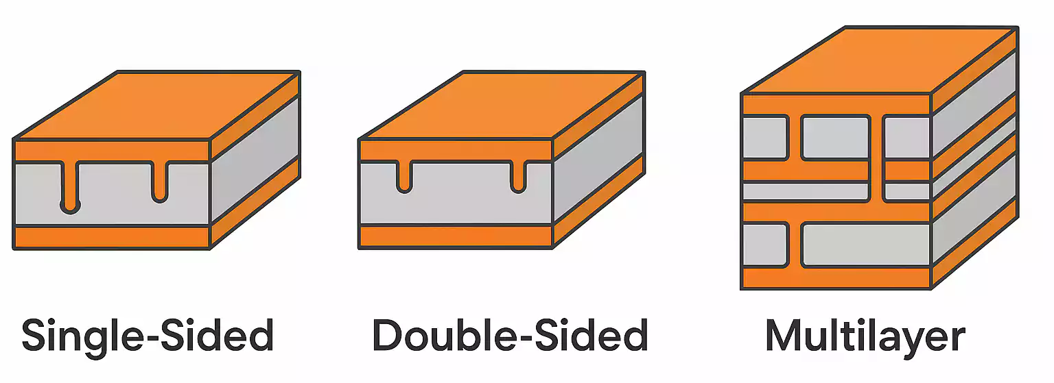
Single-sided printed circuit boards (PCBs) remain a staple in low-cost, simple electronics due to their straightforward construction and manufacturing ease. These boards feature conductive traces on only one side of the substrate, with the opposite side typically serving as a ground or insulator. While ideal for basic applications like consumer gadgets and control panels, single-sided PCBs face significant challenges in high-frequency circuits operating above 1 GHz. Engineers often encounter issues with single-sided PCB high frequency performance, where signal integrity degrades rapidly. This article delves into these limitations, focusing on signal loss, impedance mismatches, and reflections that compromise circuit reliability. Understanding these constraints helps designers make informed choices for demanding RF and microwave applications.
Understanding Single-Sided PCBs and High-Frequency Demands
Single-sided PCBs consist of a single copper layer etched onto a non-conductive substrate like FR-4, with through-hole vias limited to component mounting. In contrast, high-frequency circuits require precise control over electromagnetic wave propagation to minimize distortions. Frequencies from hundreds of MHz to several GHz demand transmission lines that behave predictably, akin to microstrip or stripline structures found in multi-layer boards. Single-sided designs lack the embedded ground planes essential for such control, leading to inconsistent single-sided PCB high frequency performance. Factory processes for these boards prioritize volume production over precision etching, which exacerbates issues in RF environments. As circuits push toward 5G, radar, and wireless communications, the simplicity of single-sided PCBs becomes a liability rather than an asset.
Core Limitations: Signal Loss in Single-Sided PCBs
Single-sided PCB signal loss emerges as a primary concern in high-frequency operations due to the absence of shielding and ground reference planes. Without a dedicated ground layer, traces act as unbalanced transmission lines, radiating energy into the air and substrate, which increases attenuation. Dielectric losses in the substrate compound this, as FR-4 materials exhibit higher dissipation factors at GHz frequencies compared to specialized low-loss laminates. Traces on single-sided boards often require longer routing paths to avoid components, further amplifying resistive and radiative losses. Engineers observe measurable degradation in signal amplitude, with attenuation rates escalating nonlinearly with frequency. IPC-6012E outlines qualification criteria for rigid boards, emphasizing surface finish and copper weight that influence loss, yet single-sided constructions rarely meet stringent RF margins.
Manufacturing tolerances play a critical role here, as variations in trace width and substrate thickness directly impact loss tangents. Factories producing single-sided PCBs adhere to IPC-A-600K acceptability standards for visual and dimensional checks, but these do not address high-frequency dielectric uniformity. In practice, signals weaken over distances as short as a few centimeters, rendering single-sided boards unsuitable for amplifiers or antennas. Troubleshooting involves spectrum analysis to quantify loss, often revealing harmonics exacerbated by poor isolation. Designers must weigh these factors against cost savings, recognizing when signal loss thresholds demand upgrades.
Related Reading: From Prototype to Production: Scaling Single-Sided Assembly for Mass Manufacturing
Challenges with Impedance Control on Single-Sided PCBs
Single-sided PCB impedance control proves notoriously difficult because traces float without a ground plane to form a controlled transmission line geometry. Characteristic impedance depends on trace width, substrate height, and dielectric constant, but single-sided layouts cannot replicate the precise spacing of microstrip lines. Variations in etching processes lead to width inconsistencies of 10-20%, causing impedance mismatches that degrade performance. At high frequencies, even minor deviations result in standing waves and power loss. Factories struggle to maintain tolerances below 10% for single-sided boards, unlike the tighter controls in multi-layer production. This limitation forces engineers to compromise on matching networks, often requiring external components that add complexity.
Practical impedance calculations for single-sided traces rely on approximate formulas, but real-world substrate variations introduce errors. JEDEC J-STD-020E addresses handling sensitivities that indirectly affect assembly, yet it underscores the fragility of single-sided boards in controlled environments. Engineers mitigate this through wider traces or serpentine patterns, but these increase inductance and loss. In high-frequency prototypes, time-domain reflectometry reveals mismatches propagating reflections back to the source. Ultimately, single-sided PCB impedance control demands unrealistic precision from standard manufacturing, pushing designs toward double-sided or multi-layer alternatives.
Signal Reflection Issues in Single-Sided High-Frequency Designs
Single-sided PCB signal reflection arises from discontinuities like vias, bends, and terminations lacking proper grounding. Without a continuous ground plane, return currents spread across the board, creating loop inductances that reflect incident waves. At high frequencies, these reflections cause ringing, overshoot, and eye diagram closure, severely impacting data rates. Trace stubs from component pads act as resonant elements, amplifying voltage standing wave ratios (VSWR). Factories etch single-sided boards with standard tolerances per IPC standards, but RF discontinuities exceed acceptable levels for GHz signals. Reflections not only attenuate desired signals but also generate electromagnetic interference (EMI) coupling to adjacent traces.
Reflection coefficients can reach 0.5 or higher due to uncharacteristic impedances, far from the ideal 50 ohms. Engineers detect these via vector network analyzers, observing S11 parameters exceeding -10 dB. Mitigation strategies include beveling corners and minimizing vias, yet single-sided constraints limit effectiveness. In factory testing, boards pass DC continuity but fail RF sweep tests, highlighting the disconnect. Single-sided PCB signal reflection thus dictates avoidance in precision RF chains, favoring layered boards with via stitching.
Related Reading: The Ultimate Guide to Component Placement in Single-Sided PCB Assembly
Practical Strategies and When to Transition Beyond Single-Sided PCBs
Engineers should assess single-sided viability early using signal integrity simulations, prioritizing applications below 500 MHz. For higher frequencies, transition to double-sided boards introduces ground planes for better single-sided PCB high frequency performance analogs. Factory-driven best practices include specifying low-loss substrates and enhanced copper foils during quoting. Adhere to IPC guidelines for trace routing, avoiding sharp angles that induce reflections. Prototyping with vector network analysis confirms limits before scaling. When signal loss or impedance exceeds 20% of budget, multi-layer designs become essential.
In troubleshooting, isolate issues by segmenting traces and measuring individually. Collaborate with manufacturers on etch factor controls to refine impedance. For legacy single-sided upgrades, overlay shielding films offer partial relief but add costs. Cost-benefit analysis reveals multi-layer premiums pay off in yield and reliability. Standards like IPC-6012E guide qualification, ensuring transitions maintain compliance.
Conclusion
Single-sided PCBs excel in simplicity but falter in high-frequency circuits due to inherent signal loss, poor impedance control, and rampant reflections. These limitations stem from lacking ground planes and precise geometries, amplifying at GHz ranges. Factory insights underscore manufacturing tolerances as key bottlenecks, aligned with IPC and JEDEC standards. Engineers benefit from early simulations and layered alternatives for robust performance. By recognizing these constraints, designs achieve optimal signal integrity without unnecessary complexity.
FAQs
Q1: What causes high single-sided PCB signal loss at high frequencies?
A1: Single-sided PCB signal loss stems from radiative energy escape without ground planes, plus dielectric dissipation in substrates like FR-4. Traces radiate as unbalanced lines, increasing attenuation with frequency. Manufacturing variations in copper thickness worsen resistive losses. Engineers measure this via insertion loss tests, often exceeding 1 dB/cm at 2 GHz. Transition to low-loss materials helps marginally.
Q2: How does single-sided PCB impedance control impact RF designs?
A2: Single-sided PCB impedance control suffers from floating traces lacking ground reference, leading to 10-20% variations. This causes mismatches, standing waves, and power loss in high-frequency paths. Factories maintain basic tolerances per IPC-A-600K, but RF needs tighter specs. Simulations predict 50-ohm targets, yet real boards deviate. Double-sided upgrades enable microstrip control.
Q3: Why is single-sided PCB signal reflection a problem in high-speed circuits?
A3: Single-sided PCB signal reflection occurs at discontinuities like vias and bends due to loop inductances from absent ground planes. Reflections generate ringing and EMI, closing eye diagrams. VSWR rises above 2:1 easily. Factory etching follows standards but ignores RF stubs. Use TDR for detection and minimize bends for mitigation.
Q4: Can single-sided PCBs handle frequencies above 1 GHz effectively?
A4: No, single-sided PCB high frequency performance degrades sharply above 1 GHz from loss, impedance issues, and reflections. Lacking shielding, they suit only low-power, short-trace apps. Standards like IPC-6012E qualify general boards, not RF. Multi-layer with ground planes are standard for GHz reliability.
References
[IPC-6012E — Qualification and Performance Specification for Rigid Printed Boards. IPC, 2017]
[IPC-A-600K — Acceptability of Printed Boards. IPC, 2020]
[JEDEC J-STD-020E — Moisture/Reflow Sensitivity Classification. JEDEC, 2014]


