 ALLPCB


Introduction
Polytetrafluoroethylene, commonly known as PTFE, serves as a premier material for printed circuit boards in high-frequency applications. Electrical engineers specify PTFE PCBs for their exceptional electrical properties, particularly the PTFE PCB dielectric constant and PTFE PCB loss tangent, which enable superior signal performance. These properties minimize signal distortion and attenuation in environments demanding precision, such as radar systems and telecommunications. Unlike standard epoxy-based laminates, PTFE maintains stability across wide frequency ranges and temperatures, making it indispensable for modern high-speed designs. Understanding these characteristics allows engineers to optimize board layouts for impedance control and reduced losses. This article delves into the fundamentals, measurement, and practical implications of PTFE PCB electrical properties.
Defining Dielectric Constant and Loss Tangent in PTFE PCBs
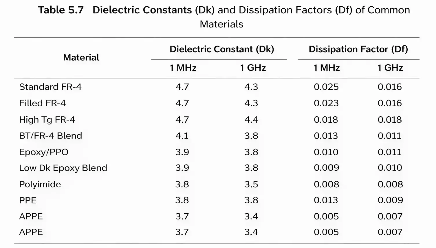
The dielectric constant, denoted as Dk or relative permittivity εr, quantifies a material's ability to store electrical energy in an electric field. In PTFE PCBs, the dielectric constant typically ranges from 2.1 to 2.6, significantly lower than the 4.2 to 4.8 found in common epoxy laminates. This low PTFE PCB dielectric constant results in faster signal propagation speeds, as velocity is inversely proportional to the square root of Dk. Engineers calculate propagation delay using formulas like t_pd = sqrt(εr) * L / c, where L is length and c is the speed of light. A stable Dk ensures predictable timing in multilayer stacks.
Loss tangent, or dissipation factor Df (tan δ), measures the energy dissipated as heat in the dielectric during signal transmission. For PTFE materials, Df values fall between 0.0002 and 0.002 at frequencies up to 10 GHz, far superior to higher-loss alternatives. This low PTFE PCB loss tangent reduces insertion loss, preserving signal amplitude over long traces. The ratio Df = ε'' / ε', where ε'' is the imaginary permittivity component, highlights inefficiency in energy storage. In high-frequency designs, even small Df increases can degrade performance, emphasizing PTFE's value.
Why PTFE PCB Electrical Properties Matter for High-Frequency Designs
Low PTFE PCB dielectric constant accelerates signal travel, reducing phase skew between traces in differential pairs. This proves critical in applications exceeding 10 GHz, where timing mismatches cause bit errors. Engineers benefit from compact layouts, as lower Dk permits wider traces for the same characteristic impedance. Combined with minimal PTFE PCB loss tangent, these traits cut power consumption and heat generation in dense boards.
Signal integrity hinges on these properties during transitions to higher data rates. PTFE's stability prevents resonance issues from Dk variations, unlike materials with frequency-dependent shifts. Factory-driven insights reveal that consistent electrical properties align with qualification under IPC-6012 standards, ensuring reliability in production volumes. Electrical engineers thus prioritize PTFE for phased array antennas and 5G infrastructure.
Moisture absorption further underscores PTFE's advantages, with uptake below 0.02 percent versus higher rates in epoxies. This maintains Dk and Df under humid conditions, vital for outdoor deployments. Overall, these PTFE PCB electrical properties drive performance in demanding sectors.
Factors Influencing PTFE PCB Dielectric Constant and Loss Tangent
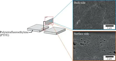
Frequency dependence affects Dk minimally in pure PTFE, remaining near 2.1 from DC to millimeter waves. Composites with glass reinforcement may elevate Dk to 2.2 through 3.5 while retaining low Df. Engineers model this using effective permittivity in stackups, accounting for weave patterns. Temperature coefficients stay low, typically 100 to 200 ppm per degree Celsius, preserving properties up to 260 degrees Celsius.
Loss tangent exhibits slight increases at higher frequencies due to molecular relaxation, but values under 0.001 suit most RF needs. Fabrication fillers like ceramics can adjust Df for specific bandwidths. Moisture minimally impacts PTFE, unlike hydrophilic resins, stabilizing long-term performance.
Measurement adheres to IPC-TM-650 procedures, such as the stripline method for precise Dk and Df extraction. These tests use vector network analyzers on coupons cut from production panels. Validation confirms material specs before full qualification.
Measuring and Specifying PTFE PCB Dielectric Constant and Loss Tangent
Engineers employ split-post dielectric resonators or coaxial probes per IPC-TM-650 2.5.5 series methods to quantify Dk and Df. These techniques isolate material contributions from conductor losses, yielding process and design values. Process Dk reflects fabricated boards, while design Dk aids simulation. Consistency between measurements ensures impedance matches simulations.
Frequency sweeps from 1 MHz to 40 GHz reveal PTFE's flat response, guiding material selection. Temperature chambers during testing simulate operational extremes. Standards like IPC-4103 define specs for high-speed laminates, specifying tolerances such as Dk ±0.05.
Design Best Practices for Optimizing PTFE PCB Electrical Properties
Control characteristic impedance Z0 = (87 / sqrt(εr + 1.41)) * log(5.98h / (0.8w + t)) for microstrips, leveraging low Dk for finer lines. Multilayer designs stack PTFE cores with compatible bond plies to minimize Df interfaces. Simulate with field solvers incorporating measured Dk and Df for accurate S-parameters.
Fabrication demands specialized processes: plasma drilling for vias, sodium etch for adhesion. Specify low-profile copper to reduce skin effect losses. Bake boards pre-assembly to desorb trace moisture, stabilizing properties.
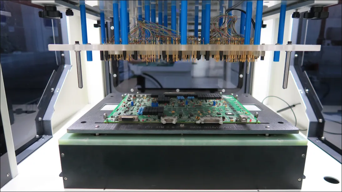
Qualification per IPC-6012 verifies electrical performance post-fabrication. Electrical engineers document Dk/Df in datasheets, correlating to TDR measurements.
Common Challenges and Troubleshooting in PTFE PCBs
Unexpected loss spikes often trace to contamination raising Df. Inspect for particulates via ionic testing. Dk drift signals delamination; ultrasound C-scans detect voids.
Fabrication warpage from CTE mismatch requires constrained lamination. Adjust press cycles per material guidelines.
Conclusion
PTFE PCB materials excel through their low dielectric constant and loss tangent, delivering unmatched performance in high-frequency realms. Electrical engineers harness these properties for precise control, low attenuation, and reliability. Adhering to standards ensures reproducible outcomes from design to deployment. Selecting and processing PTFE thoughtfully unlocks its full potential in next-generation electronics.
FAQs
Q1: What is the typical PTFE PCB dielectric constant, and why does it matter?
A1: The PTFE PCB dielectric constant typically ranges from 2.1 to 2.6, enabling faster signal speeds and compact designs compared to higher-Dk materials. This low value reduces propagation delay, critical for synchronizing high-speed signals in RF applications. Stability across frequencies minimizes simulation-to-hardware discrepancies. Engineers specify it for impedance-controlled layouts in 5G and radar boards.
Q2: How does PTFE PCB loss tangent affect high-frequency performance?
A2: PTFE PCB loss tangent, often 0.0002 to 0.002, quantifies dielectric energy loss, directly impacting signal attenuation. Lower values preserve amplitude over distance, essential beyond 10 GHz. Compared to epoxies, this cuts insertion loss by orders of magnitude. Factory tests per standards confirm values for production confidence. Monitor via VNA sweeps during qualification.
Q3: What factors influence PTFE PCB electrical properties during manufacturing?
A3: PTFE PCB electrical properties like dielectric constant and loss tangent vary with fillers, temperature, and moisture. Glass reinforcement slightly raises Dk while maintaining low Df. Processing controls, such as baking, prevent absorption effects. Adhere to IPC guidelines for consistent outcomes. Simulate stackups accounting for these variables.
Q4: How do you measure PTFE PCB dielectric constant and loss tangent accurately?
A4: Use IPC-TM-650 stripline or resonator methods with network analyzers for precise PTFE PCB dielectric constant and loss tangent. Test at operational frequencies and temperatures. Extract effective values from TRL calibration. Correlate with board-level TDR for validation. This ensures design margins align with fabricated performance.
References
IPC-TM-650 — Test Methods Manual for Printed Boards and Assemblies. IPC
IPC-4103 — Specification for Base Materials for High Speed/High Frequency Printed Boards. IPC
IPC-6012E — Qualification and Performance Specification for Rigid Printed Boards. IPC, 2017





