ALLPCB


As wearable devices evolve from exercise assistants and entertainment tools to health companions, photoplethysmography (PPG) measurement of heart rate (HR), blood oxygen saturation (SpO2), and other biometric indicators has become an essential function.
The key design challenge is how to develop a high-precision, reliable PPG measurement solution that meets product requirements and, where needed, clinical-level expectations.
This article presents multiple PPG measurement designs for wearable devices to address common engineering requirements.
PPG Principles for Heart Rate and Blood Oxygen Measurement
A typical PPG measurement system consists of a light emitter (light-emitting diode, LED), a light sensor (photodiode, PD), an analog front end (AFE) chip, and an accelerometer. The accelerometer provides motion data that is combined with optical signals as input to signal processing algorithms.
PPG detection emits light into the skin and measures the resulting variations in received light intensity. The AFE converts the analog signal to a digital signal to obtain the raw PPG waveform. Motion data from the accelerometer is used by algorithms to improve robustness under movement.
Heart rate measurement using PPG relies on the fact that blood volume in peripheral tissue varies pulsatilely with cardiac activity. The photodiode senses these pulsatile changes in light intensity. The AFE conditions and converts this optical signal into an electrical waveform, from which heart rate is calculated.
SpO2 measurement uses the different absorption spectra of oxyhemoglobin and deoxyhemoglobin at red (660 nm) and infrared (940 nm) wavelengths. By measuring the relative absorption at these wavelengths, the device can continuously estimate blood oxygen saturation from the PPG signal.
PPG Optical Path Structure and Process Design
The accuracy of PPG-derived metrics depends strongly on the quality and stability of the raw signal, which in turn is determined by the optical path structure. A well-designed optical path and manufacturing process are foundational for achieving high-precision PPG detection in wearable products.
Optical path design typically covers optical sub-board layout, light window design, and related structural process choices. The transmission path through the PD and LED light windows and the stack-up structure (LEDs oriented along the arm direction) are important considerations. Figure 1 illustrates the typical PPG optical path direction.
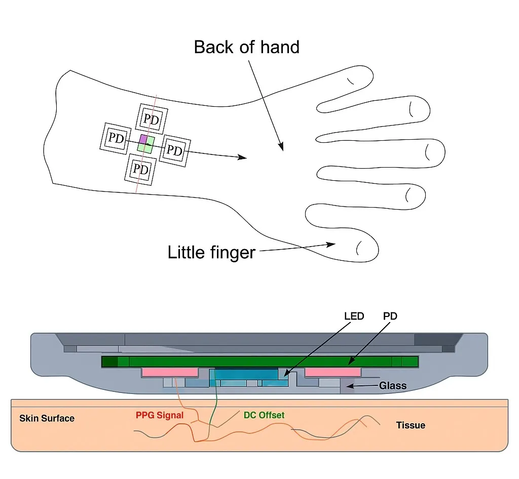
Figure 1 Schematic of PPG optical path direction in a wearable device
Design goals for optical path structure include ensuring the optical window conforms closely to the skin, minimizing ambient light interference, and reducing direct emission light that reaches the PD without passing through the intended tissue volume.
1. Optical Sub-board Layouts
Typically, the optical layout center (often the raised platform center) coincides with the device center. For green LEDs used in heart rate measurement, the center-to-PD spacing (gd) is recommended at 3.8–4.5 mm, with a preferred value of 3.8 mm. For red and infrared LEDs used for SpO2, the center-to-PD spacing (rd) is recommended at 5.5–7.5 mm, with a preferred value of 6.6 mm. Common layout patterns include:
Cross layout: The layout center is symmetric, placing two tri-color LEDs around the center with PDs distributed evenly around them, as shown in Figure 2.
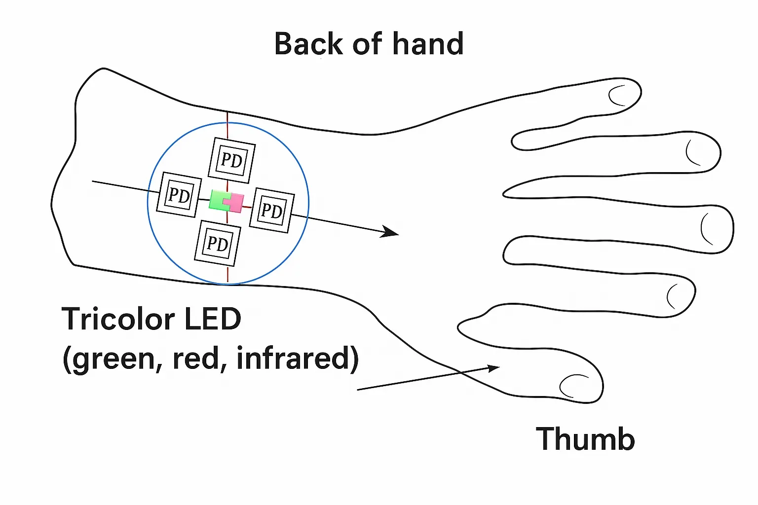
Figure 2 Cross optical layout schematic for product application
T layout: Place PD near the layout center, with two green LEDs symmetrically distributed along the strap direction around the PD. The red/IR LEDs for SpO2 are positioned on the perpendicular bisector of the line between the two green LEDs.
Linear layout A: Use the midpoint of the line connecting the PD center and the SpO2 LED optical center as the layout center. Along the strap direction, place PD, green LED, and SpO2 LED in sequence.
Linear layout B: Use the midpoint of the line connecting the green LED optical center and the SpO2 LED optical center as the layout center. Place green and SpO2 LEDs along the strap direction with the PD positioned between them.
2. Light Window Design Schemes
There are two common light window design schemes: two-shot molded light windows and silk-screened lens light windows.
Two-shot molded light window: This approach uses two-shot injection molding to integrate the transparent light window with the opaque housing in a single part, as illustrated in Figure 6. Two-shot molding reduces stray light and yields a mechanically stable structure, but increases mold cost.
Figure 6 Two-shot molded light window schematic
Silk-screened lens light window: This scheme attaches one or more lenses to the housing. The underside of each lens has a silk-printed black ink region that blocks light where not required; light passes through the transparent window regions to form the prescribed optical paths. The structure is shown in Figure 7.
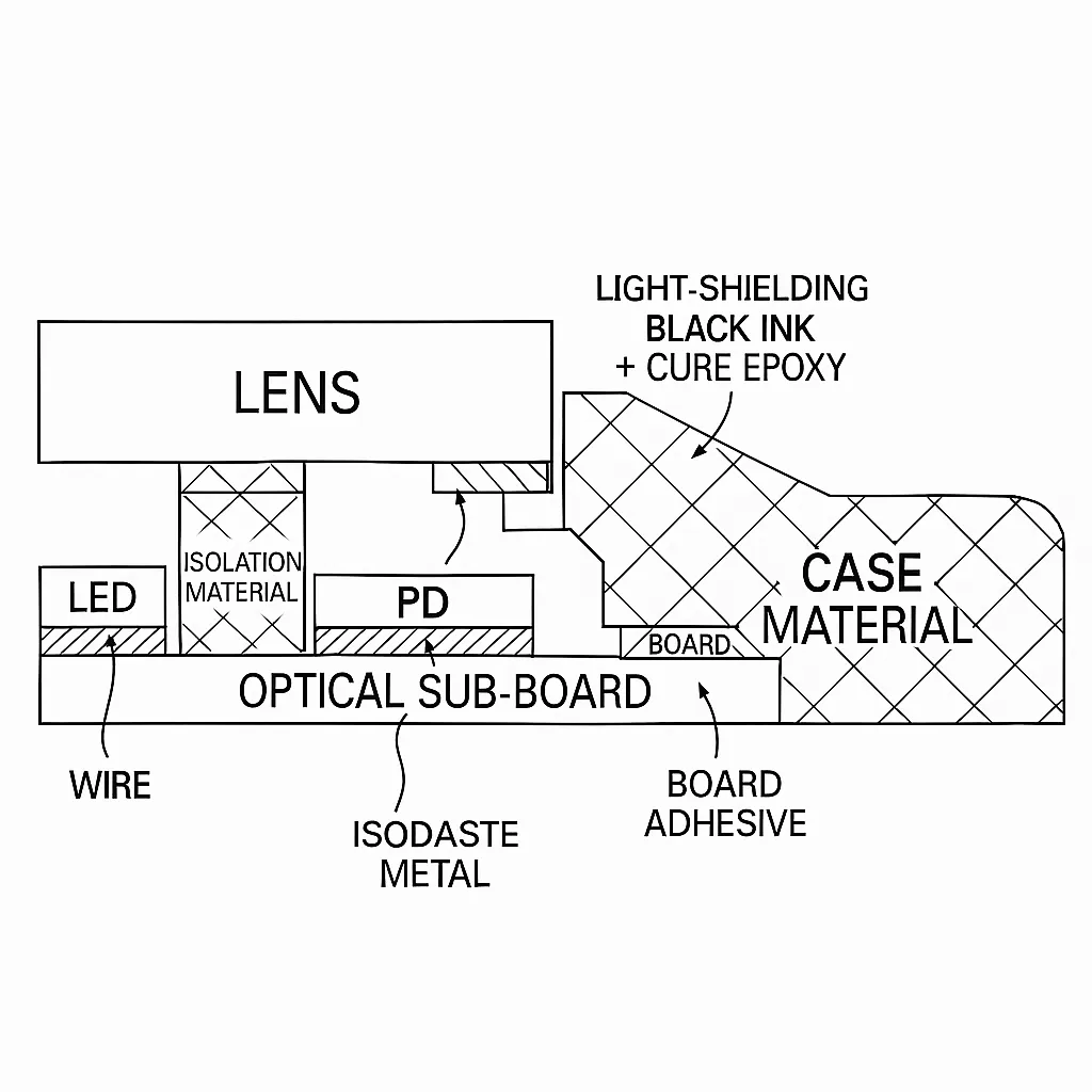
Figure 7 Silk-screened lens light window schematic
Because the lens material is transparent, to reduce direct light transmission from an LED window to the PD window, it is recommended to apply anti-reflective or light-shaping features (for example, Fresnel textures) on the inner surface of the LED window to increase optical efficiency. The PD window inner surface can also use Fresnel textures for light focusing and enhanced transmission.
Conclusion
Even with an optimized optical structure and process, achieving the system's full performance potential depends on the use of a high-quality analog front end (AFE) and appropriate signal processing algorithms.