ALLPCB


Overview
This article discusses the application of audio power amplifiers in wearable devices and common design challenges encountered when selecting amplifiers for these products.
Part 1 — Common challenges when selecting amplifiers for wearables
01 Insufficient output power
Many amplifier chips marketed for wearable devices list ratings such as 3 W or 5 W in their datasheets. In practice, a device marked 3 W often measures closer to 1 W, and one marked 5 W may only reach about 2 W. Such optimistic specifications complicate hardware development and can significantly extend project schedules.
02 Package size too large
Wearable devices have very limited internal space. Amplifier chips in larger packages such as SOP-8 occupy considerable PCB area, making it difficult to reduce overall board size.
03 High shutdown current
Wearables typically use small-capacity lithium batteries. If an amplifier has a high shutdown current, it will noticeably reduce device standby time.
04 Poor immunity to interference and degraded audio quality
Small PCB layouts in wearable devices make them more susceptible to high-frequency interference. Amplifiers with weak EMI immunity can generate audible noise, degrading perceived audio quality.
Part 2 — AD8107 design objectives and features
Design motivation
The AD8107 was designed to address the issues above for smart wearables and children’s learning devices, focusing on realistic application requirements and simplified implementation.
Key features
- High output power: At 1 kHz and 5 V supply, AD8107 can deliver up to 3 W into 3 Ω with THD+N < 10%, and 2 W into 3 Ω with THD+N < 1%.
- Simple application circuit: The typical application requires only three capacitors and two resistors.
- Small package: DFN8L 2×2 package; includes thermal protection.
- Wide supply range: 2.0 V to 5.5 V. Shutdown current < 1 μA.
- Improved EMI immunity: Layout optimizations for high-frequency wireless environments.
Part 3 — AD8107 technical description
Product overview
AD8107 is an AB-class, mono, shutdown-capable, bridged audio power amplifier. With a 1 kHz input and 5 V supply, maximum drive power is 3 W into 3 Ω at THD < 10%, and 2 W into 3 Ω at THD < 1%. Total harmonic distortion plus noise across the audio band is less than 1% (20 Hz to 20 kHz).
The device requires a minimal number of external components while providing high-quality output. AD8107 output stages do not require external coupling capacitors, boost capacitors, buffer networks, or external feedback resistors in typical bridged applications.
Product advantages
- Sufficient output power with low distortion.
- Strong immunity to interference.
- Wide supply range and low shutdown current.
- Simple application with few external components.
- Small DFN8 package with thermal protection.
Typical applications
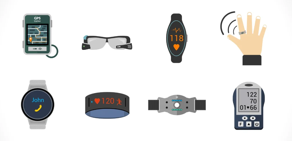
- Smart wearable devices
- Children's smart learning devices and learning pens
- Tablet computers
- Home security and monitoring devices
Internal block diagram
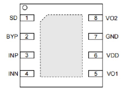
Pin definition
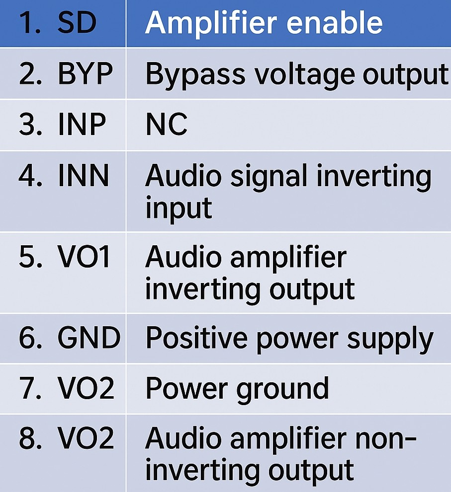
Pin description
Typical application circuit

Component descriptions for the application circuit
Ri: Input resistor that, together with Rf, sets the closed-loop gain. Ri also forms a high-pass filter with Ci; the cutoff frequency is fC = 1/(2πRiCi).
Ci: Input coupling capacitor. It blocks DC at the amplifier input and forms a high-pass filter with Ri; fC = 1/(2πRiCi).
Rf: Feedback resistor used with Ri to set the closed-loop gain.
Cs: Power supply bypass capacitor that provides decoupling for the power rail.
CB: Bypass capacitor for the VDD/2 reference node.
Part 4 — AD8107 application notes
1. Bridged output configuration
Internally, AD8107 contains two amplifier stages with slightly different structures. The input stage gain is set externally, while the output stage is internally configured for unity inversion. The closed-loop gain of the input stage is set by Rf and Ri, whereas the output stage gain is fixed by two internal resistors. The input stage output feeds the output stage, producing two outputs of equal amplitude and 180° phase difference. Therefore, the overall gain is AVD = 2 * (Rf / Ri).
When a load is connected between VO1 and VO2, the amplifier operates in a bridged mode. Compared with single-ended operation where the load is referenced to ground, the bridged mode doubles the output amplitude for a given input and can produce up to four times the output power under the same supply and load conditions. This increases output power without requiring higher current from a single output node.
For headphone and small speaker applications, bridged outputs avoid DC at the load center point because both outputs reference VDD/2. This removes the need for large output coupling capacitors required in single-ended single-supply designs. Omitting the coupling capacitor in single-ended layouts would leave VDD/2 present across the load, increasing internal power dissipation and potentially damaging the speaker. Large coupling capacitors, such as 470 μF with an 8 Ω load, form a high-pass filter that limits low-frequency response, so designers must balance PCB size, cost, and low-frequency performance.
2. Power supply bypassing
Proper power supply bypassing is critical for low-noise performance and supply filtering. Bypass capacitors on the Bypass and VDD pins should be placed close to the chip. Increasing bulk bypass capacitance can improve low-frequency THD+N but also affects supply stability. A typical bypass scheme uses 10 μF and 0.1 μF capacitors on a 5 V supply to stabilize the rail. The choice of bypass capacitor values depends on trade-offs among low-frequency THD+N, system cost, and board size.
3. Shutdown function
AD8107 provides an SD pin to disable amplifier bias circuits to reduce power consumption when the device is not in use. Driving the SD pin high activates shutdown: internal power switches disconnect power to the amplifiers, and the input, output, and internal bias outputs go to 0 V. Typical shutdown static current is 1 μA. In many systems, SD is driven by a microcontroller pin for fast, clean transitions. Alternatively, a single-pole switch and a pull-up resistor can be used: when the switch is closed, SD is pulled to ground and the amplifier operates; when open, SD is driven high into shutdown.
Note: AD8107 does not include internal pull-up or pull-down resistors on the SD pin. The SD pin voltage must be defined externally. Leaving SD floating can result in undefined logic levels and unpredictable amplifier behavior, so do not leave this pin unconnected in application designs.
4. Selection of the bias capacitor CB
Internally, the two amplifier stages share a VDD/2 DC bias. The CB capacitor determines the time constant for the bias to reach VDD/2 during power-up or when SD transitions from high to low. A smaller CB charges more quickly, allowing the amplifiers to reach normal operation faster. However, if CB is too small, the reference voltage will track supply ripple more closely and increase noise, degrading audio quality. If CB is too large, the bias charge time increases, so the amplifier will take longer to enter normal operation after SD is released. If audio is applied immediately after pulling SD low, some initial audio may be missed. Selecting an appropriate CB value balances startup time and audio performance.