ALLPCB


Introduction
Microvia PCB materials play a critical role in high-density interconnect (HDI) designs where compact layouts demand reliable interconnections. Engineers face challenges in balancing thermal stresses from assembly processes with the need for pristine signal transmission at high speeds. Selecting the right laminates ensures microvia integrity amid reflow soldering and operational heat cycles. This article explores HDI PCB laminates optimized for microvia PCB thermal management and signal performance. Factory insights reveal how material choices prevent common failures like via cracking or signal distortion. Understanding these factors empowers electric engineers to specify robust builds.
What Are Microvia PCB Materials and Why Do They Matter?
Microvia PCB materials refer to the dielectric laminates and cores that form the substrate for laser-drilled vias under 150 microns in diameter. These materials enable stacked or staggered microvias in HDI structures, packing more routing density into smaller footprints. In modern electronics, from smartphones to servers, HDI boards rely on microvias to connect fine-pitch components without compromising board space. Poor material selection leads to reliability issues, such as warpage or delamination during thermal excursions. Signal integrity suffers if the dielectric alters propagation speeds or introduces losses. Factory-driven perspectives emphasize matching laminate properties to process capabilities for consistent yields.
The relevance intensifies with rising clock rates and power densities. Microvia PCB materials must withstand multiple lamination cycles while maintaining electrical stability. Engineers prioritize laminates that support laser ablation without residue, ensuring clean via walls for plating. Thermal mismatches exacerbate stresses in stacked vias, potentially causing opens after assembly. By focusing on proven properties, designs align with manufacturing realities, reducing iterations.
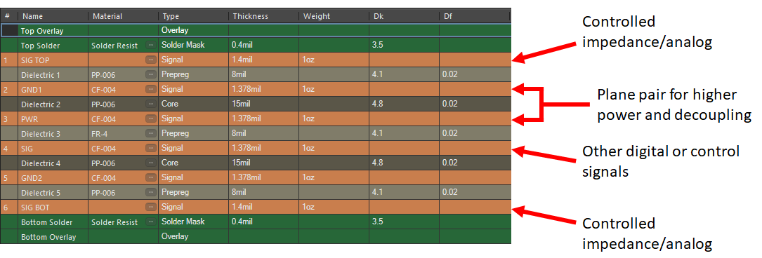
Key Material Properties for Microvia PCBs
Laminates for microvia PCBs demand specific attributes for thermal stability and signal integrity. Coefficient of thermal expansion (CTE) in the Z-axis proves vital, as it governs via barrel integrity under heat. Materials with controlled CTE minimize differential expansion against copper, preventing cracks in stacked configurations. Glass transition temperature (Tg) indicates the point where the resin softens, so higher values support lead-free soldering profiles. Dielectric constant (Dk) influences impedance control, while low dissipation factor (Df) curbs attenuation in high-frequency paths.
Factory testing per IPC-2226 guidelines verifies these properties during qualification. Low moisture absorption complements thermal management by stabilizing Dk under humidity. Resin systems like epoxy blends or advanced fillers tune these traits for microvia demands. Signal paths benefit from stable Dk across frequencies, avoiding skew in differential pairs. Balancing these ensures microvia PCB thermal management aligns with electrical goals.
Related Reading: PCB Microvia Material Selection: Impact on Performance and Reliability
Technical Principles of Thermal Stability in Microvia PCB Materials
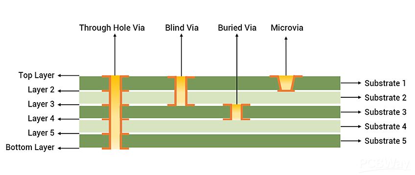
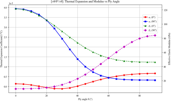
Thermal stability hinges on how laminates respond to temperature gradients during fabrication and use. Sequential lamination builds HDI layers, exposing microvias to repeated presses at elevated temperatures. Laminates with symmetric CTE across axes reduce warpage, maintaining planarity for fine-line imaging. Z-axis expansion dominates via reliability, as mismatches induce shear at copper-dielectric interfaces. IPC/JPCA-4104 specifications outline test methods for CTE and Tg, guiding material validation.
Heat dissipation pathways form through filled vias and copper planes, but substrate conductivity matters too. Low thermal resistance laminates aid microvia PCB thermal management by spreading heat evenly. During reflow, rapid ramps stress microvias; stable materials resist barrel cracking. Factory simulations predict these behaviors using thermal-mechanical models. Engineers select based on operating envelopes, ensuring margins for excursions.
Degradation mechanisms like resin charring or filler migration undermine long-term performance. High Tg laminates shift the transition above process peaks, preserving modulus. Combined with low CTE, they form the backbone of reliable HDI stackups.
Signal Integrity Considerations and Microvia PCB Dielectric Constant
Signal integrity in microvia PCBs relies on dielectric properties that preserve waveform fidelity. Microvia PCB dielectric constant dictates phase velocity and crosstalk coupling. Consistent Dk values prevent timing errors in high-speed buses. Low Df materials attenuate less, critical for multi-gigabit rates where insertion loss accumulates. Factory characterization measures these at operating frequencies to confirm suitability.
Microvias introduce stubs if not back-drilled, altering effective Dk. Laminates with low variation versus frequency maintain controlled impedance. Stacked vias demand uniform dielectric fill for consistent propagation. Engineers model these interactions early, selecting HDI PCB laminates that match simulation assumptions. Poor choices amplify jitter or eye closure.
Resin homogeneity ensures microvia walls contribute minimally to loss. Advanced fillers stabilize properties under thermal cycling, linking back to CTE control.
Related Reading: Microvia Materials: Selecting the Right Dielectric for Optimal Performance
Best Practices for Selecting HDI PCB Laminates
Start with application demands: frequency, power, and thermal budget dictate laminate class. For microvia PCB CTE matching, prioritize Z-axis values close to copper foil expansion. Consult datasheets for laser drillability, as UV or CO2 compatibility affects via taper. Verify Tg exceeds peak reflow by margin for process robustness. IPC-6012 performance specs frame qualification tests like thermal shock.
Layer stackup influences choices; thinner cores suit anylayer HDI but need low CTE for stacking. Balance cost with performance, opting for resin-coated copper (RCC) in build-up layers. Factory trials assess via fill and plating adhesion post-lamination. Simulate warpage using CTE data for asymmetric builds.
- CTE (Z-axis): Via reliability - Match to copper, low post-Tg rise
- Dk/Df: Signal propagation - Low and stable at target frequency
- Tg: Thermal process window - Above soldering peak
- Moisture Absorption: Dk stability - Below 0.5% for humidity exposure
- Laser Drillability: Clean via formation - Compatible with drill wavelength
Conduct via chain testing per standards to validate. Collaborate with fabricators for material availability and process windows.
Microvia PCB Thermal Management Strategies
Effective microvia PCB thermal management integrates laminate selection with layout. Low CTE HDI PCB laminates reduce thermomechanical stress in dense arrays. Embed thermal vias near hotspots, leveraging microvia density for conduction. Copper balance across layers counters warpage from CTE asymmetry. Factory bake-outs precondition boards, minimizing popcorn effects.
Advanced resins enhance through-plane conductivity without raising Dk. Monitor junction temperatures via modeling, iterating laminate choices. Sequential builds allow hybrid stacks, using high-Tg cores with low-CTE build-ups.
Reliability testing cycles boards through JEDEC profiles, confirming microvia survival.
Conclusion
Selecting microvia PCB materials demands a holistic view of thermal stability and signal integrity. HDI PCB laminates with optimized CTE, Dk, and Tg form the foundation for reliable designs. Factory-aligned practices, guided by IPC standards, bridge engineering intent with manufacturability. Engineers gain confidence by prioritizing these properties early. Future HDI evolutions will lean on even tighter material controls. Robust choices ensure performance in demanding applications.
FAQs
Q1: What role does microvia PCB CTE play in HDI reliability?
A1: Microvia PCB CTE governs expansion matching between dielectric and copper during thermal cycles. Low Z-axis CTE prevents via barrel cracking in stacked structures, as per IPC-2226 guidelines. Factory lamination stresses highlight this, where mismatches cause delamination. Selecting laminates with stable CTE across temperatures ensures long-term integrity under operational heat.
Q2: How does microvia PCB dielectric constant affect signal integrity?
A2: Microvia PCB dielectric constant determines signal velocity and impedance in high-speed paths. Stable, low Dk values minimize skew and crosstalk in dense routing. Variations with frequency or moisture degrade eye diagrams. Engineers choose HDI PCB laminates tested for consistency to maintain performance margins.
Q3: Why prioritize thermal stability in microvia PCB materials?
A3: Thermal stability in microvia PCB materials withstands reflow and cycling without compromising vias. High Tg and low CTE laminates resist warpage and cracking. IPC/JPCA-4104 tests validate these for sequential builds. Factory insights stress this for yield in complex HDI.
Q4: What are best practices for HDI PCB laminates in microvia designs?
A4: Prioritize laser-drillable HDI PCB laminates with low CTE and Df for thermal and signal needs. Verify via IPC standards during qualification. Balance stackup symmetry and conduct thermal simulations. Collaborate on process windows for optimal results.
References
IPC-2226A — Sectional Design Standard for High Density Interconnect Printed Boards. IPC, 2003
IPC/JPCA-4104 — Specification for Base Materials for High Density Interconnect (HDI) Printed Boards. IPC, latest revision
IPC-6012DS — Qualification and Performance Specification for High Density Interconnect (HDI) Printed Boards. IPC, 2015