 ALLPCB


Are you a hobbyist looking to level up your PCB design skills? Understanding PCB impedance control is a key step to ensuring your circuits work reliably, especially when dealing with high-speed signals. In this guide, we’ll break down the basics of PCB impedance control in an easy way, share practical PCB design tips for beginners, and offer signal integrity DIY PCB advice to help you avoid common pitfalls. Let’s dive into the details and make this complex topic simple and actionable for your next project!
What Is PCB Impedance Control and Why Does It Matter?
PCB impedance control refers to managing the electrical resistance and reactance along the traces of a printed circuit board (PCB) to ensure signals travel without distortion. Think of it like a highway for data—if the road isn’t smooth or the lanes aren’t the right width, cars (signals) can crash or slow down. For hobbyists working on projects with high-speed signals, like USB, HDMI, or RF circuits, impedance mismatches can cause data errors, noise, or complete signal failure.
Impedance is measured in ohms (Ω), and common values for controlled impedance are 50Ω for single-ended traces (like in RF designs) and 100Ω for differential pairs (like in USB or Ethernet). Without proper control, signals can reflect back along the trace, creating interference and degrading performance. For beginners, mastering this concept is a game-changer for building reliable, high-performing PCBs.
The Basics of Impedance in PCB Design
Impedance isn’t just about resistance; it’s a combination of resistance, capacitance, and inductance that affects how signals behave on a PCB. Here’s a simple breakdown of the factors that influence impedance:
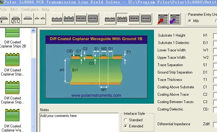
- Trace Width: Wider traces have lower impedance, while narrower traces have higher impedance. For a 50Ω impedance on a standard FR-4 board, a trace width of around 6-10 mils (0.15-0.25 mm) is common, depending on the board’s thickness and dielectric constant.
- Trace Thickness: Thicker copper traces reduce resistance, slightly lowering impedance. Standard copper thickness is 1 oz/ft2 (35 μm), but high-current designs might use 2 oz/ft2.
- Dielectric Material: The PCB substrate (often FR-4) has a dielectric constant (Dk) that affects impedance. FR-4 typically has a Dk of 4.2-4.5, which hobbyists should consider when calculating trace dimensions.
- Trace Length and Spacing: Longer traces or closely spaced traces can introduce unwanted capacitance or crosstalk, impacting impedance.
For hobbyists, the goal is to match the impedance of your traces to the requirements of your components or communication protocol. This ensures signals arrive at their destination without distortion or loss.
Why Hobbyists Should Care About Signal Integrity
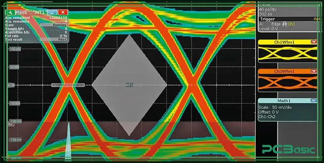
Signal integrity refers to the quality of an electrical signal as it travels through your PCB. Poor signal integrity can lead to data corruption, timing errors, or electromagnetic interference (EMI). As a hobbyist, you might not be designing cutting-edge 5G hardware, but even simple projects like an Arduino-based sensor with a high-speed communication line can suffer from signal issues if impedance isn’t controlled.
For example, if you’re building a USB device, mismatched impedance can cause data packets to fail, leading to connection drops. By focusing on signal integrity DIY PCB techniques, you can avoid these headaches and create more reliable designs.
PCB Impedance Control Made Easy for Beginners
Impedance control might sound intimidating, but with the right approach, it’s manageable even for hobbyists. Here are some easy steps to get started:
1. Know Your Design Requirements
Start by checking the specifications of the components or protocols you’re using. For instance, USB 2.0 requires a differential impedance of 90Ω ± 15%, while many RF applications need 50Ω single-ended impedance. Write down these target values before designing your PCB.
2. Use Online Calculators for Trace Dimensions
As a beginner, you don’t need to do complex math to figure out trace widths and spacing. Free online tools can calculate the dimensions for you based on your target impedance, board material, and layer stack-up. Input values like dielectric constant (Dk), board thickness (often 1.6 mm for standard PCBs), and copper weight to get accurate results.
3. Stick to a Consistent Layer Stack-Up
For hobbyist projects, a 2-layer or 4-layer PCB is usually enough. Keep your signal traces on the top layer and use the bottom layer as a ground plane to minimize interference. A solid ground plane helps maintain consistent impedance by providing a return path for signals.
4. Route Traces Carefully
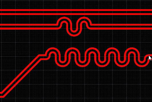
Avoid sharp bends in high-speed traces, as they can cause signal reflections. Use 45-degree angles or smooth curves instead. Also, keep high-speed traces as short as possible to reduce the chance of impedance issues.
5. Test and Iterate
Once your PCB is manufactured, test it with an oscilloscope if possible. Look for signal distortions or ringing (oscillations after a signal transition). If you spot issues, adjust your trace widths or spacing in the next revision of your design.
PCB Design Tips for Beginners to Master Impedance Control
Here are some practical PCB design tips for beginners to ensure impedance control and signal integrity in your projects:
- Choose the Right Board Material: For most hobbyist projects, FR-4 is fine and cost-effective. However, if you’re working on very high-frequency designs (above 1 GHz), consider materials with a lower dielectric constant for better signal performance.
- Maintain Uniform Trace Widths: If a trace changes width along its path, it can cause an impedance mismatch. Keep widths consistent for high-speed signals.
- Use Ground Planes: A continuous ground plane under your signal traces helps stabilize impedance and reduces EMI. Avoid splitting the ground plane unless absolutely necessary.
- Space Differential Pairs Properly: For protocols like USB or Ethernet, route differential pairs (two traces carrying complementary signals) close together with equal lengths to maintain impedance and minimize noise.
- Avoid Overloading Vias: Vias (holes connecting layers) can introduce inductance and affect impedance. Minimize their use on high-speed traces or add extra vias for current return paths if needed.
By following these tips, you’ll build a strong foundation for creating PCBs with better signal integrity, even as a beginner.
Common Mistakes to Avoid in Signal Integrity DIY PCB Projects
Even with the best intentions, hobbyists often make mistakes that hurt signal integrity. Here are some pitfalls to watch out for:
- Ignoring Impedance Requirements: Not checking the impedance needs of your components or protocol can lead to signal issues. Always start with the specs.
- Routing Over Split Planes: Running a high-speed trace over a split in the ground plane disrupts the return path, causing impedance mismatches and noise.
- Using Incorrect Trace Widths: Guessing trace widths instead of calculating them can result in impedance values far from your target. Use a calculator to get it right.
- Neglecting Termination Resistors: For very high-speed signals, termination resistors (placed at the end of a trace) can prevent reflections. Research if your design needs them.
Avoiding these errors will save you time and frustration when debugging your PCB designs.
Tools and Resources for Hobbyists to Simplify Impedance Control
You don’t need expensive software or equipment to get started with impedance control. Here are some accessible tools and resources for hobbyists:
- Free PCB Design Software: Many open-source or free tools offer basic features for routing traces and setting up layer stack-ups. Look for software with built-in impedance calculators or plugins.
- Online Impedance Calculators: Websites provide free calculators for determining trace widths and spacing based on your target impedance and board parameters.
- Community Forums: Online communities for electronics enthusiasts often have threads on signal integrity and impedance control. Search for advice or share your designs for feedback.
- Basic Testing Equipment: If you can invest in a low-cost oscilloscope (under $100), it’s a great way to visualize signal behavior and spot impedance issues.
These resources make PCB impedance control easy and accessible, even if you’re just starting out.
How to Work with Manufacturers for Controlled Impedance
As a hobbyist, you might not have the tools to measure impedance directly, but many PCB manufacturers offer controlled impedance services at a reasonable cost. Here’s how to ensure your design is fabricated correctly:
- Specify Impedance Requirements: Clearly note the target impedance values (e.g., 50Ω for single-ended traces) in your design files or fabrication notes.
- Provide Stack-Up Details: Share your layer stack-up (number of layers, material, thickness) so the manufacturer can adjust their process to meet your impedance needs.
- Request Test Coupons: Some manufacturers include test coupons (small test structures on the PCB panel) to verify impedance after fabrication. This is especially useful for critical designs.
Communicating clearly with your manufacturer ensures your PCB meets the necessary impedance standards without guesswork.
Final Thoughts on PCB Impedance Control for Hobbyists
Mastering PCB impedance control might seem daunting at first, but with the right knowledge and tools, it’s within reach for any hobbyist. By understanding the basics of impedance, following simple PCB design tips for beginners, and applying signal integrity DIY PCB techniques, you can create reliable, high-performing circuit boards for your projects. Start small, use online resources to calculate trace dimensions, and don’t hesitate to test and revise your designs as you learn.
Whether you’re building a simple microcontroller project or experimenting with high-speed communication protocols, impedance control is a skill that will set your work apart. Keep experimenting, stay curious, and enjoy the process of bringing your electronic ideas to life!


