ALLPCB


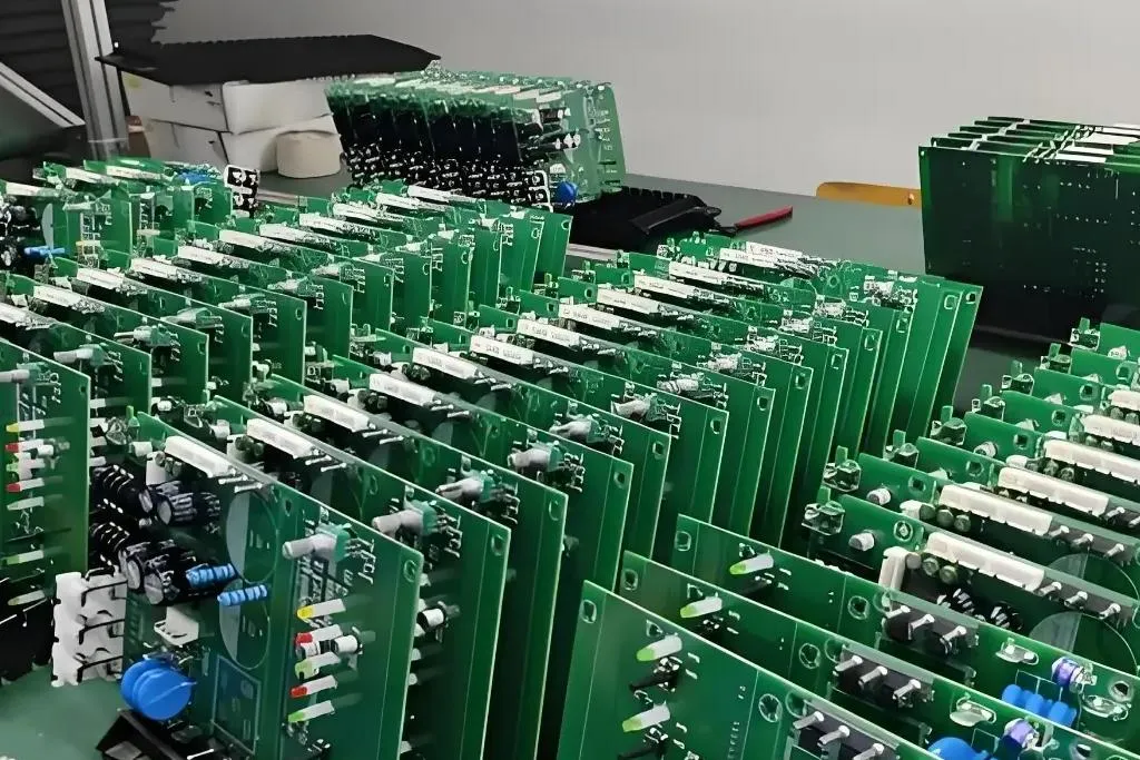
In the fast-paced world of electronics manufacturing, printed circuit board (PCB) defects can lead to significant financial losses, delayed production schedules, and damaged reputations. For companies engaged in mass production, the stakes are even higher. The hidden costs of PCB defects are often underestimated, but with proper quality control measures, these issues can be minimized. This blog explores the impact of PCB defects in mass production and provides actionable strategies for mastering quality control, including techniques like automated optical inspection (AOI) and X-ray inspection for PCB assembly.
Whether you're looking to improve PCB defect analysis in mass production or implement robust quality control in PCB manufacturing, this guide offers practical insights to help you prevent defects and ensure reliability in high-volume production. Let’s dive into the details of how defects affect your bottom line and the proven methods to tackle them.
Understanding the Hidden Costs of PCB Defects in Mass Production
PCB defects might seem like a small issue at first glance, but their impact can ripple through the entire production process, especially in high-volume manufacturing. These hidden costs often go beyond the price of replacing a faulty board. They include wasted materials, labor hours spent on rework, delayed shipments, and even potential recalls if defective products reach customers. For businesses focused on preventing PCB defects in high volume, understanding these costs is the first step to mitigating them.
Consider this: a single defect in a batch of 10,000 PCBs could lead to a failure rate of just 0.01%. While that percentage seems minor, it translates to 100 defective units. If each unit costs $50 to produce, that’s a direct loss of $5,000—before factoring in the cost of identifying the issue, scrapping or reworking the boards, and addressing customer complaints. Add in potential downtime on a production line running at 1,000 units per hour, and a few hours of delay could cost thousands more in lost output.
Beyond financial losses, defects can harm a company’s reputation. If defective PCBs lead to malfunctioning end products, customers may lose trust, impacting future sales. In industries like automotive or medical devices, where reliability is critical, a single defect could have catastrophic consequences, leading to legal liabilities or safety concerns.
The Root Causes of PCB Defects in High-Volume Production
To master quality control in PCB manufacturing, it’s essential to identify the common causes of defects during mass production. These issues often stem from design flaws, material inconsistencies, or process errors. Here are some of the most frequent culprits:
- Design Errors: Incorrect trace widths or improper spacing can lead to signal integrity issues or shorts. For instance, a trace width of 0.2mm might be too narrow for a high-current application, causing overheating and failure.
- Material Issues: Low-quality substrates or inconsistent copper thickness can result in delamination or poor conductivity. A copper layer below the standard 1oz/ft2 might not handle the required current, leading to breakdowns.
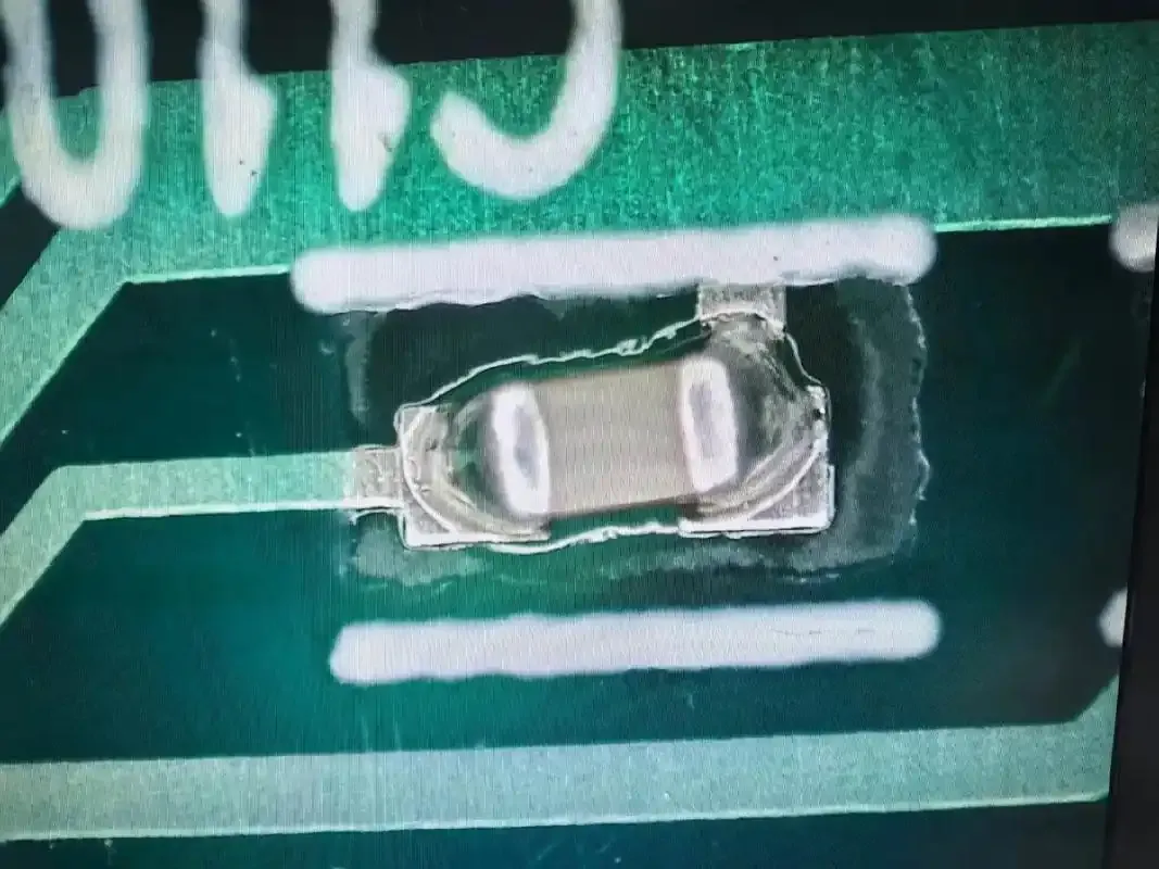
- Manufacturing Mishaps: Misalignment during component placement or insufficient soldering can cause open circuits or weak joints. In high-speed production, even a 0.1mm misalignment can lead to connectivity issues.
- Environmental Factors: Dust, humidity, or temperature fluctuations in the production facility can introduce contaminants or affect soldering quality, leading to defects like corrosion over time.
Identifying these root causes through PCB defect analysis in mass production allows manufacturers to address issues before they escalate. The earlier a defect is caught, the lower the cost of correction. This is where advanced inspection techniques come into play.
The Role of Quality Control in Preventing PCB Defects
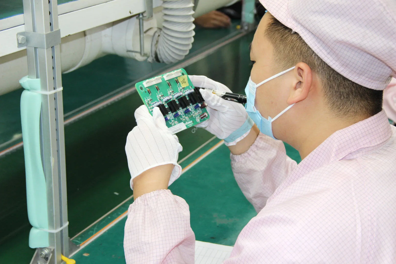
Effective quality control in PCB manufacturing is the backbone of defect prevention, especially in high-volume production. Quality control isn’t just about catching defects after they occur—it’s about building processes that minimize the risk of defects in the first place. This involves a combination of rigorous design validation, material selection, process optimization, and inspection techniques.
For instance, implementing strict incoming material checks can prevent the use of substandard substrates or components. Similarly, optimizing soldering parameters—such as maintaining a reflow oven temperature profile between 220°C and 260°C for lead-free solder—can reduce the likelihood of cold joints or tombstoning. However, even with the best preventive measures, some defects may still slip through. That’s why inspection methods like AOI and X-ray are critical in mass production.
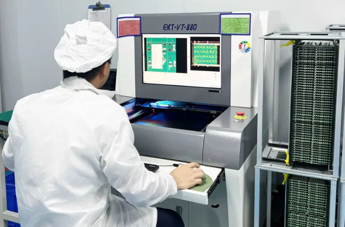
Automated Optical Inspection (AOI) in PCB Mass Production
One of the most effective tools for AOI PCB mass production is Automated Optical Inspection. AOI uses high-resolution cameras and advanced imaging software to detect surface-level defects on PCBs. This technology is particularly valuable in high-volume settings because of its speed and accuracy.
AOI systems can scan thousands of PCBs per hour, identifying issues like missing components, incorrect placements, or soldering defects. For example, an AOI machine can detect a misaligned resistor with a deviation as small as 0.05mm, flagging it for correction before it moves to the next production stage. This rapid detection minimizes the number of defective units that progress down the line, saving time and resources.
The benefits of AOI include:
- Speed: AOI can inspect a PCB in seconds, keeping up with the pace of mass production lines running at 500-1,000 units per hour.
- Accuracy: Modern AOI systems achieve defect detection rates of over 99%, reducing false positives and ensuring reliability.
- Cost-Effectiveness: By catching defects early, AOI prevents costly rework or scrap later in the process.
However, AOI has limitations. It can only inspect visible surfaces, meaning internal defects or issues beneath components remain undetected. This is where complementary methods like X-ray inspection become essential.
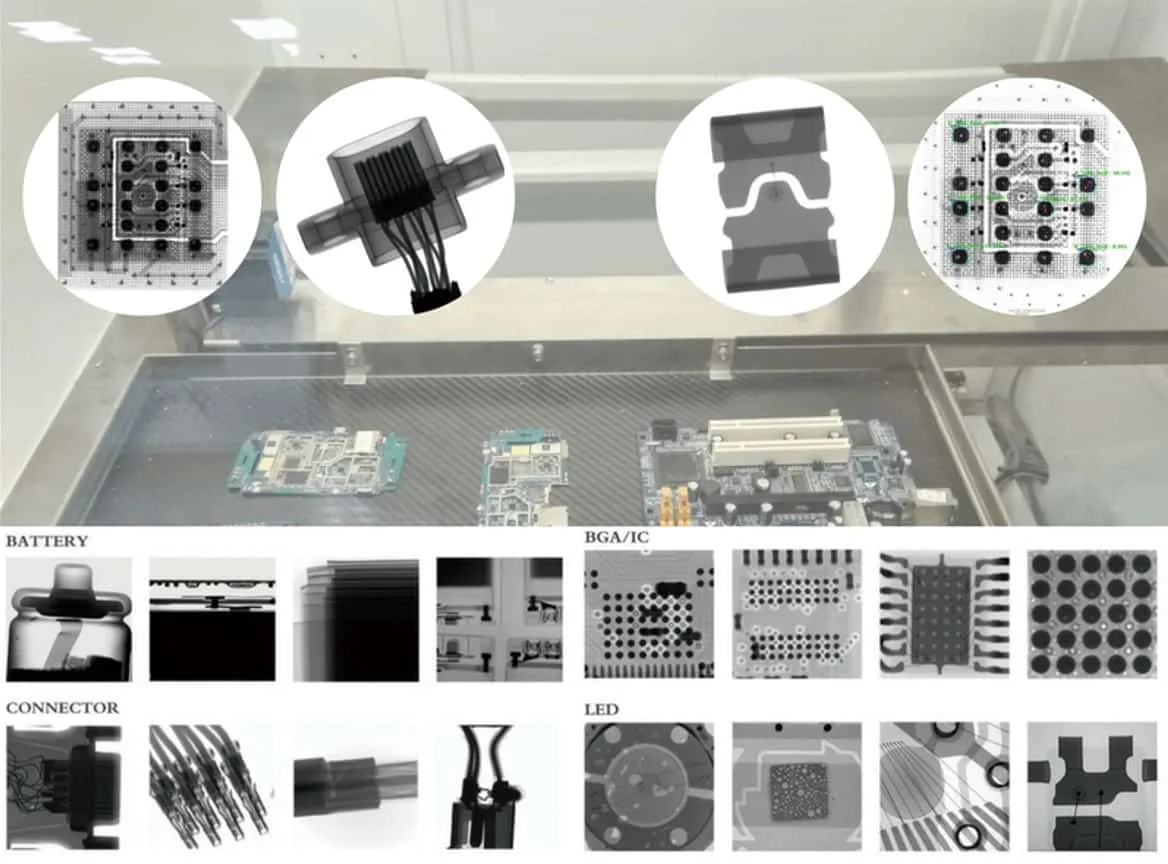
X-Ray Inspection for PCB Assembly: Uncovering Hidden Defects
For a deeper level of defect detection, X-ray inspection in PCB assembly is a game-changer. Unlike AOI, X-ray systems penetrate the PCB to reveal internal structures, making them ideal for identifying hidden issues such as voids in solder joints, misaligned vias, or defects in multi-layer boards.
In high-volume production, X-ray inspection is often used selectively on complex assemblies or after AOI has flagged potential issues. For instance, in a multi-layer PCB with buried vias, an X-ray system can detect a void in a solder ball under a Ball Grid Array (BGA) component—a defect that could cause intermittent failures if undetected. Modern X-ray systems can achieve resolutions down to 1 micrometer, ensuring even the smallest anomalies are caught.
Key advantages of X-ray inspection include:
- Non-Destructive Testing: X-ray inspection doesn’t damage the PCB, allowing for further testing or use if no defects are found.
- Internal Visibility: It reveals issues inside the board or under components, which AOI cannot detect.
- Precision: High-resolution imaging ensures accurate identification of defects, reducing the risk of false negatives.
While X-ray inspection is slower and more expensive than AOI, its ability to uncover hidden defects makes it indispensable for critical applications in industries like aerospace or medical devices.
Strategies for Preventing PCB Defects in High Volume
While inspection tools like AOI and X-ray are vital, preventing PCB defects in high volume starts long before inspection. Here are actionable strategies to reduce defect rates in mass production:
- Design for Manufacturability (DFM): Optimize PCB designs to minimize manufacturing challenges. For example, ensure trace widths are at least 0.25mm for standard processes to avoid etching issues, and maintain a minimum clearance of 0.2mm between components to prevent soldering defects.
- Standardized Processes: Implement consistent manufacturing protocols, such as maintaining a stencil thickness of 0.1-0.15mm for solder paste application to ensure uniform deposits.
- Material Quality: Source high-grade materials with verified specifications. A substrate with a dielectric constant of 4.5 and a loss tangent below 0.02 can ensure better signal integrity in high-frequency applications.
- Operator Training: Train staff to recognize and address common issues, such as improper handling that could introduce static damage to sensitive components.
- Real-Time Monitoring: Use sensors and data analytics to monitor production parameters like temperature or humidity, ensuring they stay within acceptable ranges (e.g., 20-25°C and 40-60% humidity for optimal soldering conditions).
By combining these preventive measures with advanced inspection techniques, manufacturers can significantly reduce defect rates and the associated costs.
Building a Robust Quality Control Framework for Mass Production
To truly master quality control in PCB manufacturing, companies need a comprehensive framework that integrates prevention, detection, and continuous improvement. Here’s how to build one:
- Layered Inspection: Use a combination of visual checks, AOI, and X-ray inspection at different stages of production to catch defects early and thoroughly.
- Data-Driven Analysis: Collect and analyze defect data to identify patterns. If 80% of defects are due to soldering issues, focus on optimizing the reflow process or stencil design.
- Feedback Loops: Establish clear communication between design, production, and quality teams to address recurring issues. For example, if a specific component placement causes frequent misalignment, adjust the design or pick-and-place settings.
- Continuous Improvement: Regularly update processes and equipment based on the latest industry advancements to stay ahead of potential defect causes.
This multi-faceted approach ensures that quality control is not a one-time fix but an ongoing commitment to excellence in PCB defect analysis in mass production.
Conclusion: Investing in Quality for Long-Term Savings
The hidden costs of PCB defects in mass production can be staggering, from direct financial losses to damaged customer trust. However, by prioritizing quality control in PCB manufacturing and leveraging advanced tools like AOI PCB mass production systems and X-ray inspection in PCB assembly, manufacturers can drastically reduce these costs. More importantly, adopting proactive strategies for preventing PCB defects in high volume ensures consistent product reliability and long-term success.
Investing in quality control isn’t just about avoiding losses—it’s about building a reputation for excellence. By mastering defect prevention and detection, you can deliver flawless PCBs to your customers, even at the largest production scales. Start implementing these strategies today to safeguard your production line and bottom line.