 ALLPCB


In the fast-paced world of electronics manufacturing, achieving compliance with international standards while maintaining efficiency is a top priority. Standardized design using Surface Mount Technology (SMT) offers a powerful solution to meet IEC (International Electrotechnical Commission) compliance requirements. This blog explores how SMT, when integrated into a standardized design approach, can help manufacturers adhere to strict IEC guidelines, improve production efficiency, and streamline the Surface Mount Assembly Process. Whether you're an engineer or a manufacturer, you'll find practical insights to optimize your PCB design process for better results.
What Is Standardized Design with SMT and How Does It Relate to IEC Compliance?
Standardized design refers to creating uniform processes, layouts, and component selections in PCB (Printed Circuit Board) design to ensure consistency, reliability, and compliance with global standards like those set by the IEC. SMT, or Surface Mount Technology, plays a crucial role in this approach by enabling smaller, more efficient, and highly automated assembly processes. By combining SMT with standardized design practices, manufacturers can achieve IEC compliance—covering safety, performance, and environmental regulations—while reducing errors and production costs.
IEC standards, such as IEC 60950 for safety of information technology equipment or IEC 61000 for electromagnetic compatibility, often require precise control over component placement, soldering quality, and thermal management. SMT supports these needs through its precision and compatibility with automated manufacturing, making it easier to meet stringent requirements. In the sections below, we'll dive deeper into how SMT contributes to compliance and efficiency in PCB production.
Understanding Surface Mount Technology (SMT) and Its Benefits for Compliance
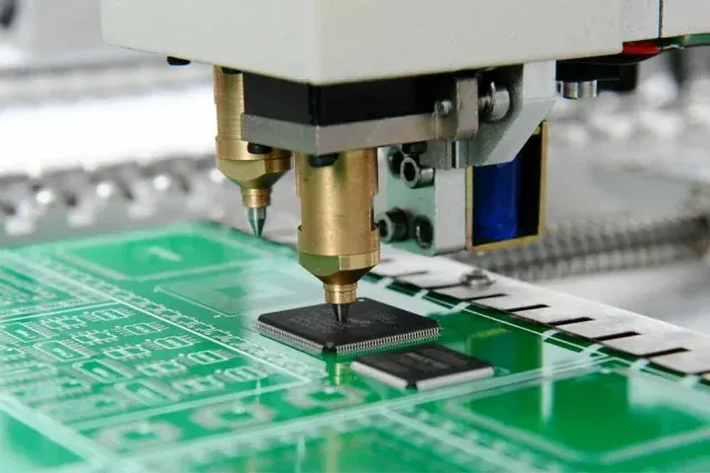
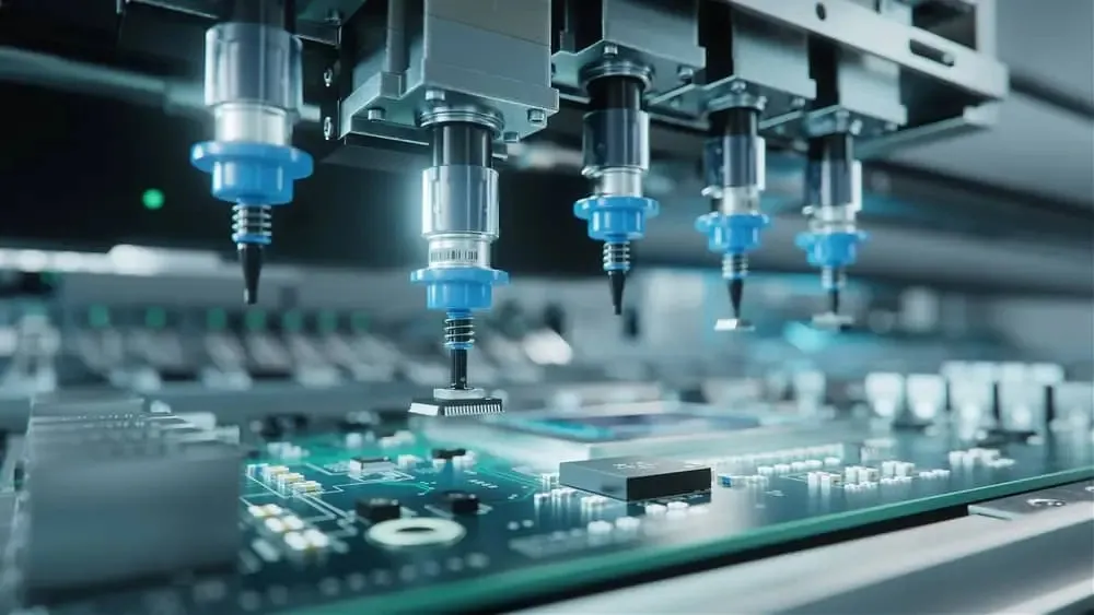
Surface Mount Technology is a method of assembling electronic components directly onto the surface of a PCB, as opposed to inserting them through holes (as in through-hole technology). This technique uses automated pick-and-place machines and reflow soldering to attach components, offering several advantages for standardized design and IEC compliance.
Key Benefits of SMT:
- Precision and Consistency: SMT allows for precise placement of components, with tolerances as tight as 0.1 mm, ensuring uniformity across batches. This precision helps meet IEC standards for electrical spacing and component alignment, reducing risks like short circuits.
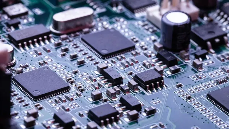
- Smaller Footprint: SMT components are typically smaller, allowing for compact designs that comply with IEC guidelines for space-constrained applications, such as in medical devices (IEC 60601).
- Automated Production: The use of automated machinery in SMT reduces human error, ensuring consistent soldering quality—a critical factor for IEC compliance in terms of reliability and safety.
- Thermal and Electrical Performance: SMT designs can achieve better thermal dissipation and lower impedance (e.g., reducing trace impedance to below 50 ohms in high-speed designs), aligning with IEC standards for electromagnetic compatibility (EMC).
How SMT Enhances the Surface Mount Assembly Process for IEC Standards
The Surface Mount Assembly Process involves several steps: solder paste application, component placement, reflow soldering, and inspection. When standardized, this process not only boosts production efficiency but also ensures adherence to IEC requirements at every stage.
1. Solder Paste Application: Using standardized stencils with precise aperture sizes (e.g., 0.005 inches thick for fine-pitch components), manufacturers can ensure uniform solder paste deposition. This reduces defects like solder bridging, which could violate IEC standards for electrical safety.
2. Component Placement: Automated pick-and-place machines in SMT can achieve placement accuracy within 0.025 mm, ensuring components are positioned correctly to meet IEC spacing and clearance rules (e.g., creepage distances as per IEC 60950).
3. Reflow Soldering: Standardized reflow profiles (e.g., peak temperatures of 245°C for lead-free solder) ensure consistent joint quality, critical for IEC reliability tests. Proper thermal management during reflow also prevents component damage, aligning with safety standards.
4. Inspection and Testing: Automated Optical Inspection (AOI) systems, commonly used in SMT, detect defects like misaligned components or insufficient solder with over 95% accuracy. This step is vital for meeting IEC quality and performance benchmarks.
By standardizing these steps, manufacturers can create repeatable processes that minimize variations, ensuring every board meets IEC criteria without costly rework.
Standardized PCB Design Techniques for IEC Compliance Using SMT
Designing a PCB with SMT in mind requires specific techniques to ensure both efficiency and compliance with IEC standards. Below are actionable strategies to incorporate into your design workflow:
1. Component Selection and Footprints: Choose SMT components with standardized footprints (e.g., following IPC-7351 guidelines) to ensure compatibility with automated assembly and IEC spacing requirements. For instance, maintain a minimum clearance of 0.5 mm between pads for low-voltage applications as per IEC 60950.
2. Trace Width and Spacing: Design traces with appropriate widths (e.g., 0.2 mm for signals carrying 1A) and spacing to handle current loads and prevent crosstalk, aligning with IEC 61000 standards for EMC. Use simulation tools to verify impedance values, targeting 50 ohms for high-speed signals.
3. Thermal Management: Incorporate thermal vias and heat sinks in SMT designs to manage temperatures, ensuring compliance with IEC thermal safety limits (e.g., maximum surface temperature of 70°C for accessible parts under IEC 60950). Place thermal vias near high-power components like voltage regulators.
4. Design for Manufacturability (DFM): Standardize layer stack-ups (e.g., 4-layer boards with 1.6 mm thickness) and panelization to optimize SMT assembly. This reduces production errors and ensures consistent performance during IEC testing.
These techniques, when applied consistently, create a robust foundation for IEC-compliant designs while simplifying the transition to large-scale production.
Improving Production Efficiency with SMT and Standardized Design
One of the standout benefits of using SMT in a standardized design framework is the significant boost to production efficiency. Here's how this combination delivers measurable results:
1. Faster Assembly Times: SMT’s compatibility with automated systems cuts assembly time by up to 50% compared to manual through-hole methods. Standardized designs further reduce setup times by eliminating the need for custom adjustments.
2. Reduced Material Waste: Standardized SMT designs optimize component placement and routing, minimizing scrap rates by as much as 30%. This efficiency also aligns with IEC environmental standards like IEC 62474 for material declarations.
3. Lower Labor Costs: Automation in SMT reduces the need for skilled manual labor, with studies showing labor cost reductions of up to 40% in high-volume production. Standardization ensures fewer errors, further cutting rework expenses.
4. Scalability: Standardized SMT designs are easily scalable, allowing manufacturers to ramp up production without sacrificing quality or compliance. For example, a standardized 4-layer PCB design can be replicated across thousands of units with consistent results.
By focusing on these efficiency gains, manufacturers can produce high-quality, IEC-compliant boards at a lower cost per unit, gaining a competitive edge in the market.
Challenges in Achieving IEC Compliance with SMT and How to Overcome Them
While SMT offers many advantages, there are challenges in aligning with IEC standards. Understanding these hurdles and their solutions is key to successful implementation.
1. Component Miniaturization Issues: As SMT components shrink (e.g., 0201 packages with dimensions of 0.6 x 0.3 mm), maintaining IEC-required clearances becomes difficult. Solution: Use design software with built-in DRC (Design Rule Check) tools to enforce minimum spacing rules automatically.
2. Thermal Stress During Reflow: High reflow temperatures (up to 260°C for lead-free solder) can stress components, risking failure under IEC reliability tests. Solution: Standardize reflow profiles and use components rated for high thermal cycles.
3. Solder Joint Reliability: Poor solder joints can fail IEC vibration or thermal shock tests (e.g., IEC 60068). Solution: Implement AOI and X-ray inspection to detect defects early, ensuring joint quality meets standards.
Addressing these challenges through standardized processes and advanced tools ensures that SMT designs remain compliant without compromising efficiency.
Case Study: Achieving IEC Compliance with SMT in a Real-World Project
Consider a project involving the design of a power supply module required to meet IEC 60950 safety standards. The design team adopted a standardized SMT approach, using 0805 resistors and capacitors for ease of assembly and consistent footprints. They maintained a creepage distance of 3.2 mm between high-voltage traces, as mandated by the standard, and used a 4-layer PCB stack-up for better signal integrity and thermal management.
During production, automated SMT assembly achieved a defect rate of less than 0.5%, thanks to standardized solder paste stencils and reflow profiles peaking at 245°C. AOI detected 98% of potential issues before testing, ensuring compliance during IEC audits. The project was completed 30% faster than a comparable through-hole design, demonstrating the efficiency of standardized SMT processes.
This example highlights how combining SMT with standardization can deliver compliant, high-quality results in less time.
Conclusion: Leveraging SMT for IEC Compliance and Efficiency
Standardized design using Surface Mount Technology offers a proven path to achieving IEC compliance while improving production efficiency. By adopting SMT in the Surface Mount Assembly Process, manufacturers benefit from precision, automation, and scalability—key factors in meeting strict international standards. From optimizing PCB layouts to streamlining assembly, the techniques and strategies discussed in this blog provide a roadmap for engineers and manufacturers to create reliable, compliant products.
Integrating SMT into your design and production workflow not only ensures adherence to IEC guidelines but also positions your operations for cost savings and faster time-to-market. As electronics continue to evolve, leveraging standardized SMT practices will remain a cornerstone of success in the industry.
 ."
."


