 ALLPCB


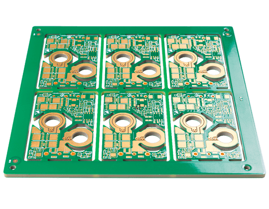
In the fast-paced world of electronics, not all printed circuit boards (PCBs) are designed to handle the same challenges. While standard PCBs work well for many devices, some applications demand more power and durability. That's where heavy copper PCBs come in. Featuring copper weights of 3 oz per square foot or more, these robust boards are built to manage high currents and extreme conditions that would overwhelm typical PCBs. From electric vehicles to industrial machinery, heavy copper PCBs are the foundation of reliable, high-performance electronics.
In this blog, we'll dive into the applications, benefits, and manufacturing best practices of heavy copper PCBs. Whether you're an engineer designing cutting-edge systems or just exploring this technology, you'll find practical insights to guide your next project.
Applications of Heavy Copper PCBs
Heavy copper PCBs shine in industries where high power and heat management are non-negotiable. Here's a look at their key applications:
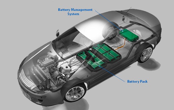
- Automotive: The rise of electric vehicles (EVs) has fueled demand for heavy copper PCBs. In battery management systems (BMS), these boards handle currents up to 100 amps or more during charging and discharging cycles. They also power distribution units (PDUs), ensuring efficient electricity flow between batteries, motors, and onboard systems. Their ability to endure temperatures exceeding 150°C and resist vibration makes them perfect for automotive environments.
- Industrial: Factories rely on heavy copper PCBs for motor drives and power supplies. For example, a motor drive controlling a 10-horsepower motor might require a PCB to manage currents of 50 amps while dissipating heat effectively. These boards keep equipment running smoothly, even in dusty or high-temperature settings.
- Aerospace and Defense: In radar systems and power converters, heavy copper PCBs deliver unmatched reliability. A radar power supply might need to handle 20 amps continuously, with copper weights up to 6 oz ensuring stability under harsh conditions like altitude changes or extreme weather.
- Renewable Energy: Solar inverters and wind turbine controls depend on heavy copper PCBs to convert and distribute power. A solar inverter handling 5 kW of power could use traces designed for 30 amps, leveraging the boards' thermal and current-carrying strengths to maximize efficiency.
- Medical: High-power medical devices, such as MRI scanners, use heavy copper PCBs to manage significant electrical loads. These boards ensure consistent performance, critical for patient safety and diagnostic accuracy.
Benefits of Using Heavy Copper PCBs
Why choose heavy copper PCBs over standard options? Here are the standout advantages:
- Improved Thermal Management: The thick copper layers act as natural heat sinks, reducing operating temperatures by up to 20% compared to standard PCBs in high-power setups. This keeps components like power transistors running cooler and longer.
- Increased Current Carrying Capacity: With wider traces—sometimes exceeding 0.5 inches—heavy copper PCBs can carry currents of 50 amps or more without overheating. This allows for compact, efficient designs in power-heavy systems.
- Enhanced Mechanical Strength: The robust copper structure strengthens plated-through holes (PTHs) and connector points, withstanding forces up to 10 times greater than standard PCBs during vibration or thermal cycling.
- Reduced Layer Count: By integrating power and control circuits on a single board, heavy copper PCBs cut down on layers. A design that might need 6 layers with standard copper could drop to 4, saving space and cost.
- Better Reliability in Harsh Environments: These boards thrive in extreme conditions, maintaining performance at temperatures above 200°C or in corrosive settings, making them ideal for industrial and aerospace use.
Manufacturing Best Practices for Heavy Copper PCBs
Producing heavy copper PCBs isn't like making standard boards—it requires precision and expertise. Here are the best practices we follow to ensure top quality:
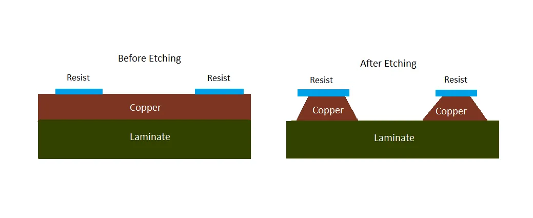
- Advanced Etching Techniques: Etching thick copper (up to 20 oz) demands control to avoid uneven traces. Differential etching, where etch rates vary across the board, achieves trace widths as tight as 0.010 inches with straight sidewalls, critical for high-current reliability.
- High-Speed Plating: Uniform copper deposition is key. High-speed plating builds layers at rates of 0.5 oz per minute, ensuring consistent thickness across traces and through-holes. This boosts electrical performance and heat transfer.
- Strict Quality Control: We use automated optical inspection (AOI) to catch defects like voids smaller than 0.005 inches, and X-ray checks to verify plating uniformity. This catches issues early, ensuring every board meets specs.
- Appropriate Substrate Selection: Substrates like high-Tg FR4 (Tg > 170°C) or polyimide handle the thermal stress of heavy copper. For a board dissipating 50 watts of heat, the right material prevents warping or delamination.
Design Considerations for Heavy Copper PCBs
Designing a heavy copper PCB requires careful planning. Here's what engineers should focus on:
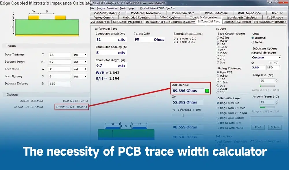
1. Trace Width and Spacing: For a 10-amp load, traces might need to be 0.050 inches wide, based on current density rules (e.g., 500 A/in²). Spacing must exceed 0.015 inches at 100 volts to prevent arcing.
2. Thermal Management: Thermal vias—say, 0.012-inch holes with 2 oz copper plating—can cut hotspot temperatures by 15°C. Thicker copper layers also spread heat, reducing reliance on external sinks.
3. Layer Stackup: A 4-layer PCB board might place power planes on outer layers with 6 oz copper and signal layers inside at 1 oz, balancing impedance (e.g., 50 ohms) and power needs.
4. Via Design: High-current paths might use 0.020-inch vias or clusters of three 0.012-inch vias, improving current flow and heat dissipation by 30% over single vias.
5. Material Selection: A substrate with a thermal conductivity of 1 W/m·K or higher supports heat dissipation in a 100-watt design, while a dielectric strength above 500 V/mil ensures insulation.
Challenges in Heavy Copper PCB Manufacturing
Heavy copper PCBs come with hurdles that require skill to overcome:
- Etching Thick Copper Layers: Removing copper up to 10 oz takes specialized chemistry and equipment. A slight over-etch could widen a 0.020-inch trace by 0.005 inches, affecting performance.
- Risk of Delamination: Thermal expansion mismatches during soldering (e.g., 260°C reflow) can stress layers. A robust substrate and controlled lamination keep risks below 1%.
- Higher Manufacturing Costs: Thicker copper and advanced processes increase costs by 20-50% over standard PCBs. For a 10x10-inch board, material alone might jump from $10 to $15.
- Limited Manufacturer Availability: Only specialized facilities handle copper weights above 6 oz. Choosing a capable partner is critical for quality and turnaround.
Partnering with ALLPCB for Heavy Copper PCB Success
Navigating the complexities of heavy copper PCBs is easier with the right manufacturer. At ALLPCB, we excel in crafting high-quality heavy copper PCBs with weights up to 15 oz. Our advanced facilities use cutting-edge etching and plating to meet your exact specs. Need to test a design fast? Our quick-turn prototyping delivers boards in as little as 48 hours. Plus, with our global logistics, your project arrives on time, anywhere in the world. Whether it's automotive, industrial, or renewable energy systems, we're here to power your success.
Conclusion
Heavy copper PCBs are the backbone of high-power electronics, delivering top-tier thermal management, current capacity, and durability. By mastering their applications, benefits, and manufacturing best practices, engineers can build systems that thrive under pressure. Yes, the process has its challenges—but the payoff in performance is worth it. With a trusted partner like ALLPCB, you can bring your heavy copper designs to life with confidence. As technology pushes forward, these boards will keep driving innovation.


