 ALLPCB


Introduction
Component replacement on multi-layer PCBs presents unique challenges for engineers working with dense electronic assemblies. Multi-layer PCB repair often requires careful handling to maintain structural integrity while restoring functionality. One of the most critical risks during these operations is PCB delamination, where layers separate due to thermal or mechanical stress. Preventing delamination demands precise control over soldering multi-layer PCBs and adherence to established thermal profiles. High temperature soldering, when mismanaged, can accelerate moisture expansion or coefficient of thermal expansion mismatches within the board stack-up. Engineers must balance repair success with long-term reliability to avoid costly failures in finished products.
What Is PCB Delamination and Why It Matters
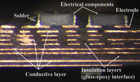
PCB delamination refers to the separation between copper layers, dielectric materials, or prepreg bonds in a multi-layer construction. This defect compromises electrical continuity and mechanical strength, often leading to intermittent connections or complete board failure under operational loads. In multi-layer PCB repair scenarios, delamination frequently occurs near component pads or vias where localized heat is applied. The issue matters because modern electronics rely on high-density interconnects that leave little margin for structural compromise. Preventing delamination preserves signal integrity and extends product lifespan in demanding environments such as automotive or industrial controls. Engineers recognize that even minor layer separation can violate performance expectations defined by industry qualification standards.
Technical Principles and Mechanisms
Delamination arises primarily from thermal stresses introduced during high temperature soldering on multi-layer PCBs. When heat is applied rapidly to a component pad, the outer copper layers expand faster than the underlying glass-reinforced epoxy, creating shear forces at the interfaces. Moisture absorbed within the laminate can vaporize at reflow temperatures, generating internal pressure that forces layers apart. Coefficient of thermal expansion mismatches between copper, resin, and glass weave further exacerbate the problem, especially in boards with eight or more layers. During multi-layer PCB repair, repeated thermal cycles from desoldering and resoldering compound these stresses. Engineers analyze these mechanisms by examining cross-sections to identify resin starvation or weave exposure as precursor conditions. Controlled ramp rates and uniform heating help mitigate the cumulative damage that leads to visible separation.
Related Reading: Delamination in Multi Layer PCBs: Diagnosing and Addressing the Root Causes of Interlayer Separation
Practical Solutions and Best Practices
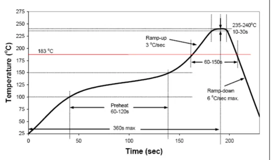
Successful component replacement on multi-layer PCBs begins with thorough preheating of the entire assembly to reduce thermal gradients. Engineers typically raise board temperature gradually to 100 to 150 degrees Celsius before applying localized heat for soldering multi-layer PCBs. This approach minimizes shock to inner layers and supports preventing delamination. Hot-air rework stations with adjustable nozzles and temperature feedback allow precise control during high temperature soldering operations. Applying flux sparingly and using low-residue formulations further reduces the risk of trapped volatiles. After replacement, a controlled cooling phase prevents rapid contraction that could reopen micro-cracks. Post-repair inspection with acoustic microscopy or thermal imaging verifies that no delamination has occurred. These steps align with qualification requirements outlined in IPC-6012E for rigid printed boards.
Related Reading: Is Your Reflow Profile Sabotaging Your PCBs? Optimizing Soldering to Prevent Delamination
Troubleshooting and Process Optimization
When delamination appears during multi-layer PCB repair, engineers first verify moisture content by baking the assembly at 125 degrees Celsius for several hours. This step removes absorbed water that would otherwise expand violently during subsequent high temperature soldering. Adjusting the soldering profile to extend soak time at intermediate temperatures allows even heat distribution through the stack-up. If separation persists near vias, engineers may reduce peak temperature or employ conductive adhesives as an alternative attachment method. Systematic documentation of each repair cycle helps identify patterns related to board thickness or copper weight. Collaboration with quality teams ensures that process adjustments remain consistent with IPC-A-600K acceptance criteria for printed boards.
Conclusion
Component replacement on multi-layer PCBs can be performed reliably when engineers prioritize thermal management and moisture control. Understanding the mechanisms behind PCB delamination enables proactive steps that protect board integrity throughout the repair process. Adopting gradual heating, verified profiles, and post-repair verification reduces the incidence of layer separation. These practices support consistent outcomes in multi-layer PCB repair while meeting performance expectations for high-reliability applications. Continued attention to soldering multi-layer PCBs and high temperature soldering parameters remains essential for long-term success.
FAQs
Q1: What causes PCB delamination during multi-layer PCB repair?
A1: Thermal shock from rapid heating and moisture vaporization inside the laminate are primary contributors. Engineers mitigate these factors by preheating assemblies and following controlled profiles that align with established qualification standards. Proper handling during high temperature soldering further reduces the likelihood of layer separation.
Q2: How can preventing delamination improve outcomes in soldering multi-layer PCBs?
A2: Preventing delamination maintains electrical continuity and mechanical strength across all layers. Uniform temperature distribution and moisture removal before rework help preserve the original board construction. These measures support reliable component attachment without introducing new defects.
Q3: What role does high temperature soldering play in multi-layer PCB repair risks?
A3: High temperature soldering introduces localized heat that can exceed the glass transition point of the dielectric material. Without adequate preheating or ramp control, this heat creates differential expansion and internal pressure. Engineers therefore monitor profiles closely to keep peak conditions within safe limits for the specific stack-up.
Q4: Which industry standards guide safe practices for component replacement on multi-layer PCBs?
A4: Standards such as JEDEC J-STD-020E address moisture sensitivity and reflow conditions that influence delamination risk. IPC-6012E provides qualification requirements for rigid boards that include thermal and mechanical performance criteria. Following these documents helps ensure repairs meet acceptance levels defined in related specifications.
References
IPC-6012E — Qualification and Performance Specification for Rigid Printed Boards. IPC, 2017
IPC-A-600K — Acceptability of Printed Boards. IPC, 2020
JEDEC J-STD-020E — Moisture/Reflow Sensitivity Classification. JEDEC, 2014


