ALLPCB


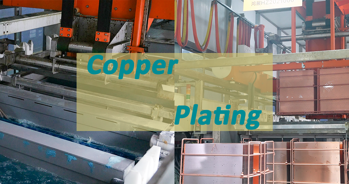
Printed Circuit Boards are the backbone of modern electronics, acting as the structural and electrical foundation for almost every electronic device. A critical step in PCB fabrication is the copper plating process, which enables the formation of electrical pathways between layers of the board. Two essential copper plating techniques used in PCB manufacturing are Electroless Copper Plating (PTH copper or chemical copper) and Electrolytic Copper Plating (also called electroplating). This article explores these two techniques, their purposes, processes, and the role they play in creating reliable and high-performance PCBs.
The Importance of Copper Plating in PCB Manufacturing
PCBs are composed of a non-conductive substrate (usually FR-4 fiberglass epoxy) laminated with thin layers of copper. During fabrication, various circuit patterns and vias (vertical interconnect access, or holes) are etched and drilled into the board. These vias need to be conductive to allow signal transmission between layers. However, since drilling removes the conductive copper, a process is needed to deposit copper inside the holes and form connections. That’s where copper plating comes into play.
Copper plating ensures:
- Electrical conductivity between layers.
- Mechanical strength of via walls.
- Surface finish suitable for component soldering.
The copper plating process typically begins with electroless copper plating, followed by electrolytic copper plating to build up the desired thickness.
Electroless Copper Plating
What is Electroless Copper Plating?
Electroless copper plating is a chemical deposition process that deposits a thin layer of copper onto non-conductive surfaces (like the walls of drilled vias) without using electricity. This is the first copper layer applied inside the holes after the board has been drilled and cleaned.
Why is it necessary?
Since the inner wall of a drilled hole is made of insulating material (FR-4), it cannot conduct electricity for electroplating. Electroless copper plating creates a thin, conductive seed layer that enables the following electroplating step.
Process Steps:
1.Cleaning and Desmearing:
After drilling, the hole walls contain debris and resin smears. A chemical cleaning process removes these contaminants and prepares the surface.
2.Conditioning:
A conditioning solution prepares the surface to accept the catalyst.
3.Catalyzation (Palladium Activation):
The board is immersed in a solution containing palladium ions. The palladium acts as a catalyst to initiate copper reduction.
4.Electroless Copper Deposition:
The board is immersed in an autocatalytic copper solution containing copper ions and a reducing agent (usually formaldehyde). The copper deposits uniformly on all exposed surfaces, including the inner walls of the vias.Key Characteristics:
- Uniform copper thickness (typically 1–2 μm).
- Essential for via conductivity.
- No electricity is required.
Challenges:
1.Requires precise chemical control.
2.Sensitive to contamination.
3.Waste treatment is necessary due to heavy metals and formaldehyde.
Electrolytic Copper Plating
What is Electrolytic Copper Plating?
Electrolytic copper plating is an electrochemical process that builds up additional copper on the conductive areas of the PCB using a direct electric current. After electroless copper has created a conductive path, electrolytic plating thickens the copper to meet mechanical and electrical requirements.
Purpose:
- Increase copper thickness in vias and on traces.
- Improve conductivity and current-carrying capacity.
- Ensure durability and reliability of connections.
Process Steps:
1.Set up:
The PCB panels are connected to a cathode (negative terminal), while copper anodes are placed in the plating bath as the positive terminal.
2.Electroplating Bath:
The board is submerged in an acidic copper sulfate solution. When electric current flows, copper ions from the anode dissolve and deposit onto the PCB’s conductive surfaces.
3.Current and Time Control:
The amount of copper deposited depends on the current density and plating time. Typical through-hole copper thickness is 20–25 μm, but high-reliability boards may require 30 μm or more.Key Characteristics:
- Uniform plating in vias and on surface features.
- Controllable copper thickness.
- Higher plating speed compared to chemical deposition.
Challenges:
- Risk of uneven plating or voids if current distribution is poor.
- Requires careful bath maintenance and process control.
- Vias with high aspect ratios are harder to plate evenly.
Key Differences Between Electroless and Electrolytic Copper Plating
Innovations and Advanced Techniques
The modern PCB design increasingly demands finer features, smaller vias (like micro vias), and high-density interconnects (HDI). As a result, traditional plating processes have been enhanced or replaced with:
- Pulse electroplating: Uses pulsed currents to improve plating in complex geometries.
- Direct metallization: Replaces palladium-based catalyzation with conductive polymers or carbon-based alternatives.
- Vertical continuous plating (VCP): Improves throughput and consistency for large-scale manufacturing.
These advancements help manufacturers meet stringent performance, environmental, and miniaturization requirements.
- Uniform plating in vias and on surface features.
- Controllable copper thickness.
- Higher plating speed compared to chemical deposition.
Conclusion
Copper plating is a critical step in PCB fabrication, bridging the gap between layers and ensuring signal integrity and mechanical robustness. Electroless copper plating forms the essential conductive base inside via holes, while electrolytic plating builds upon that foundation to meet performance specifications. Understanding both processes offers valuable insights into how high-quality PCBs are made and why they perform reliably in electronic applications ranging from consumer electronics to aerospace.
As technology continues to evolve, so will copper plating techniques, empowering PCB manufacturers to meet the ever-growing demand for smaller, faster, and more reliable electronic devices.