ALLPCB


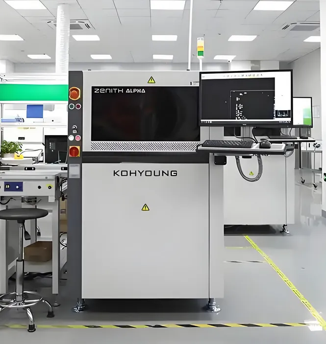
In the fast-paced world of electronics manufacturing, ensuring the quality of printed circuit boards (PCBs) is critical. Defects in PCBs can lead to product failures, costly recalls, and damaged reputations. This is where Automated Optical Inspection (AOI) steps in as a game-changer. While traditional 2D AOI has been a reliable tool for years, 3D AOI is taking defect detection to the next level with its advanced capabilities. So, how does 3D AOI compare to 2D AOI, and why is it revolutionizing PCB inspection? In short, 3D AOI offers superior precision by capturing height and depth data, enabling the detection of complex defects like poor solder joints and component misalignment that 2D systems often miss.
In this blog, we’ll dive deep into the world of advanced PCB inspection, exploring the differences between 3D AOI vs 2D AOI, the benefits of high-precision AOI systems, and specific techniques like 3D solder joint inspection and coplanarity testing. Whether you’re an engineer, manufacturer, or quality control specialist, this guide will help you understand how 3D AOI is transforming the industry.
What is Automated Optical Inspection (AOI) in PCB Manufacturing?
Automated Optical Inspection, or AOI, is a technology used to inspect PCBs for defects during the manufacturing process. Using cameras and specialized software, AOI systems scan the board to identify issues such as missing components, misalignments, and soldering errors. This non-contact method is faster and more accurate than manual inspection, making it a cornerstone of modern electronics production.
AOI systems are typically deployed at various stages of manufacturing, including after solder paste application, before and after reflow soldering, and during final assembly. By catching defects early, AOI helps reduce waste, lower production costs, and ensure that only high-quality products reach the market.
3D AOI vs 2D AOI: Understanding the Key Differences
The evolution from 2D to 3D AOI represents a significant leap in inspection technology. While both systems aim to detect defects, their approaches and capabilities differ greatly. Let’s break down the key differences between 3D AOI vs 2D AOI to understand why 3D is becoming the preferred choice for advanced PCB inspection.
1. Dimensional Analysis
2D AOI systems rely on two-dimensional imaging, capturing flat images of the PCB surface. They excel at identifying visible defects like missing components or solder bridges but struggle with issues related to height or depth. For example, a 2D system might miss a lifted component lead because it cannot measure elevation.
In contrast, 3D AOI uses advanced imaging techniques, such as laser triangulation or structured light projection, to create a three-dimensional map of the PCB. This allows the system to measure the height of components, solder joints, and other features, detecting defects that are invisible to 2D cameras. With 3D AOI, manufacturers can achieve a more comprehensive inspection, catching up to 30% more defects compared to 2D systems, according to industry studies.
2. Accuracy and Precision
High-precision AOI is critical for modern PCBs, which often feature densely packed components and fine-pitch designs. 2D AOI systems can sometimes produce false positives or negatives due to shadows, reflections, or limited viewing angles. On the other hand, 3D AOI minimizes these errors by providing a detailed view of the board’s topography, resulting in more accurate defect detection. This precision is especially valuable for complex assemblies where even a minor defect can cause significant performance issues.
3. Speed and Efficiency
While 2D AOI systems are generally faster due to simpler image processing, 3D AOI has made significant strides in recent years. Modern 3D systems use high-speed cameras and optimized algorithms to inspect boards at rates comparable to 2D systems, often processing up to 50 square centimeters per second. This balance of speed and enhanced accuracy makes 3D AOI a practical choice for high-volume production lines.
The Advantages of 3D AOI in Advanced PCB Inspection
As PCB designs become more intricate with smaller components and tighter tolerances, the need for advanced PCB inspection techniques has never been greater. 3D AOI offers several advantages that make it indispensable for manufacturers aiming to maintain high quality standards.
1. Enhanced Defect Detection
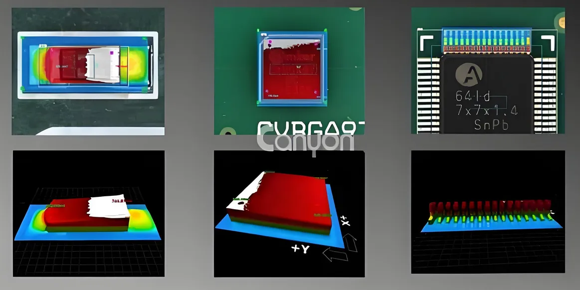
One of the standout benefits of 3D AOI is its ability to detect a wider range of defects. Beyond the surface-level issues caught by 2D systems, 3D AOI identifies problems such as insufficient solder volume, lifted leads, and component tilt. For instance, in a typical PCB with a ball grid array (BGA), 3D AOI can measure the height and shape of each solder ball, ensuring proper connection and reducing the risk of failures in the field.
2. Improved Quality Control
High-precision AOI systems like 3D AOI contribute to better overall quality control. By providing detailed data on every inspected board, these systems enable manufacturers to analyze trends, identify recurring issues, and fine-tune their processes. This data-driven approach can lead to a reduction in defect rates by as much as 40%, based on feedback from industry professionals using 3D inspection technologies.
3. Compatibility with Modern Designs
Today’s PCBs often incorporate advanced technologies like high-density interconnects (HDI) and micro-components with pitches as small as 0.4 mm. 3D AOI is uniquely suited to handle these designs, ensuring that even the smallest defects are caught before they become bigger problems. This capability is crucial for industries like aerospace and medical devices, where reliability is non-negotiable.
3D Solder Joint Inspection: A Game-Changer for Reliability
Solder joints are the backbone of any PCB, connecting components to the board and ensuring electrical conductivity. Poor solder joints can lead to intermittent connections, reduced performance, or complete failure. This is where 3D solder joint inspection shines, offering a level of detail that traditional methods cannot match.
How 3D Solder Joint Inspection Works
3D AOI systems use height measurement techniques to analyze the shape, volume, and position of solder joints. For example, laser-based 3D AOI can detect if a solder joint is concave, convex, or uneven—indicators of potential issues like cold soldering or insufficient paste. By comparing these measurements against predefined standards, the system flags defective joints with high accuracy, often achieving defect detection rates above 95%.
Benefits for PCB Manufacturing
The ability to inspect solder joints in three dimensions ensures stronger, more reliable connections. This is particularly important for surface-mount technology (SMT) components, where solder joint quality directly impacts performance. With 3D solder joint inspection, manufacturers can reduce rework costs by identifying issues early, often saving thousands of dollars per production run in high-volume environments.
Coplanarity Testing: Ensuring Component Alignment with 3D AOI
Coplanarity refers to the flatness or alignment of a component’s leads or pins relative to the PCB surface. Misaligned components can lead to poor soldering, weak connections, and mechanical stress. Coplanarity testing is a critical aspect of PCB manufacturing, and 3D AOI is the ideal tool for this task.
The Importance of Coplanarity Testing
In high-density PCB designs, even a slight deviation in coplanarity can cause significant issues. For instance, if the leads of a quad flat package (QFP) component are not level, some pins may fail to connect properly during soldering, leading to open circuits. 3D AOI measures the height of each lead with precision, often to within 10 micrometers, ensuring that all pins are within acceptable tolerances.
How 3D AOI Enhances Coplanarity Testing
Unlike 2D systems, which can only infer coplanarity based on visual cues, 3D AOI directly measures the elevation of each lead or pin. This data is used to create a detailed profile of the component’s alignment, allowing manufacturers to address issues before soldering. By integrating coplanarity testing into the inspection process, 3D AOI helps improve first-pass yields by up to 25%, as reported by industry benchmarks.
Challenges and Considerations with 3D AOI
While 3D AOI offers numerous benefits, it’s important to acknowledge some challenges associated with its adoption. Understanding these factors can help manufacturers make informed decisions about integrating high-precision AOI into their workflows.
1. Higher Initial Costs
3D AOI systems are generally more expensive than their 2D counterparts due to the advanced hardware and software required. However, the long-term savings from reduced defects and rework often justify the investment. For example, a mid-sized manufacturer might recover the cost of a 3D AOI system within 12-18 months through improved efficiency and quality.
2. Learning Curve
Implementing 3D AOI requires training for operators and engineers to interpret the detailed data and adjust inspection parameters. While this learning curve can slow initial adoption, most teams adapt within a few weeks with proper support and documentation.
3. Integration with Existing Systems
For manufacturers with established 2D AOI setups, integrating 3D systems may require updates to production lines and software. Careful planning and phased implementation can minimize disruptions, ensuring a smooth transition to advanced PCB inspection technologies.
The Future of PCB Defect Detection with 3D AOI
As electronics continue to evolve, the demand for high-precision AOI will only grow. 3D AOI is at the forefront of this transformation, driven by advancements in imaging technology, artificial intelligence, and data analytics. Future 3D AOI systems are expected to offer even faster inspection speeds, higher resolution, and seamless integration with smart manufacturing platforms.
Moreover, the rise of Industry 4.0 is pushing AOI systems to become more connected and data-driven. By storing and analyzing vast amounts of inspection data, 3D AOI can help manufacturers predict potential issues, optimize processes, and achieve near-zero defect rates. This proactive approach to quality control is set to redefine standards in PCB manufacturing.
Conclusion: Why 3D AOI is the Future of PCB Inspection
In the battle of 3D AOI vs 2D AOI, it’s clear that 3D technology offers unmatched advantages for advanced PCB inspection. From detecting complex defects with 3D solder joint inspection to ensuring perfect alignment through coplanarity testing, 3D AOI provides the precision and reliability that modern electronics demand. While the initial costs and learning curve may pose challenges, the long-term benefits of improved quality, reduced rework, and higher yields make it a worthy investment for any manufacturer.
At ALLPCB, we’re committed to staying ahead of the curve by embracing cutting-edge technologies like 3D AOI to deliver top-quality PCBs to our clients. As the industry moves toward more complex designs and stricter standards, 3D AOI will continue to play a pivotal role in ensuring flawless products. Stay tuned to our blog for more insights into the latest trends and innovations in PCB manufacturing.