 ALLPCB


In the world of printed circuit board (PCB) design, managing heat is a critical challenge. As electronic devices become smaller and more powerful, effective PCB thermal management is essential to ensure reliability and prevent failures. One often overlooked factor in inner layer heat dissipation is the role of copper thickness. So, how does copper thickness and temperature interact to influence heat dissipation in a PCB? Simply put, thicker copper layers in the inner structure of a PCB can significantly improve heat spreading and reduce hotspot temperatures, while thinner layers may struggle to handle high-power applications. In this blog, we’ll dive deep into the science behind this, explore the impact of copper thickness, and share practical tips on using thermal vias and other PCB cooling techniques to optimize performance.
Why PCB Thermal Management Matters
Heat is the enemy of electronic components. Excessive temperatures can degrade performance, cause component failure, and shorten the lifespan of a device. In high-power applications like power supplies, automotive electronics, and LED systems, managing heat is even more crucial. Poor PCB thermal management can lead to thermal stress, warping, or even complete system shutdowns. This is why understanding how heat moves through a PCB—especially through its inner layers—is vital for engineers and designers.
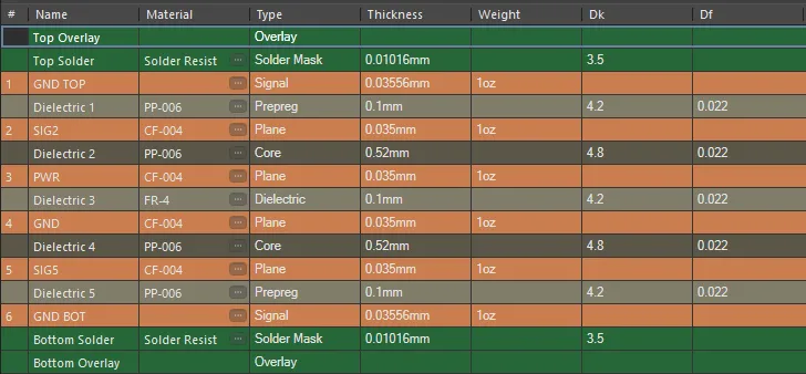
The inner layers of a multilayer PCB often play a key role in heat dissipation. While outer layers are typically exposed to air or heatsinks, inner layers rely on material properties like copper thickness to transfer heat away from critical components. Let’s explore how inner layer heat dissipation works and why copper thickness is a game-changer.
The Science of Heat Dissipation in PCBs
Heat dissipation in a PCB occurs through three main mechanisms: conduction, convection, and radiation. Conduction, the transfer of heat through materials, is the primary method in PCB design. Copper, being an excellent thermal conductor with a thermal conductivity of approximately 401 W/m·K, is the material of choice for spreading heat across a board.
In a multilayer PCB, inner copper layers act as heat spreaders. When a component generates heat, it travels through the copper layers via conduction before being dissipated to the environment through convection (air cooling) or radiation. The efficiency of this process depends heavily on the thickness of the copper in those inner layers. Thicker copper provides a larger cross-sectional area for heat to travel through, reducing thermal resistance and improving overall inner layer heat dissipation.
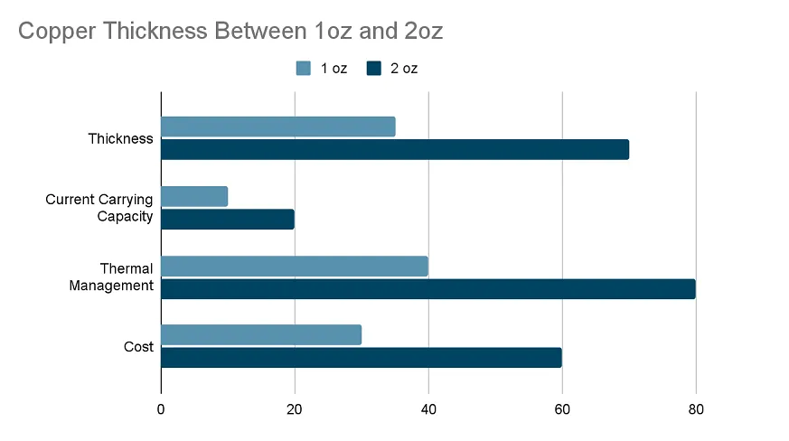
For example, a standard copper thickness of 1 oz/ft2 (about 35 micrometers) may be sufficient for low-power circuits. However, in high-power designs, using 2 oz/ft2 (70 micrometers) or even 3 oz/ft2 (105 micrometers) can lower the temperature rise by as much as 10-20°C under heavy loads, based on typical thermal simulations for power electronics.
How Copper Thickness Impacts Temperature
The relationship between copper thickness and temperature is straightforward: thicker copper layers reduce the thermal resistance of the PCB, allowing heat to spread more evenly and preventing localized hotspots. Thermal resistance, measured in °C/W, indicates how much temperature rises for a given amount of power dissipated. A lower thermal resistance means better heat dissipation.
Consider a scenario where a power IC dissipates 5 watts of heat. With a 1 oz/ft2 copper layer, the temperature rise might be around 50°C above ambient, depending on the board layout and airflow. By increasing the inner layer copper to 2 oz/ft2, the temperature rise could drop to 30-35°C due to better heat spreading. This reduction can be critical in preventing thermal failure, especially in compact designs with limited space for additional cooling solutions.
However, thicker copper isn’t always the answer. It increases manufacturing costs and can complicate the etching process for fine traces. Additionally, beyond a certain thickness (typically 3-4 oz/ft2), the benefits of further increasing copper diminish due to other limiting factors like dielectric material properties or board size. Balancing cost and performance is key when deciding on copper thickness for PCB thermal management.
The Role of Inner Layers in Multilayer PCBs
In multilayer PCBs, inner layers are often dedicated to power planes or ground planes. These planes, made of continuous copper, provide a large area for heat to spread. Unlike signal traces on outer layers, which are narrow and fragmented, inner planes can act as effective heat sinks when designed with sufficient copper thickness.
For instance, a 4-layer PCB with 2 oz/ft2 inner copper planes can handle significantly more heat than a similar board with 1 oz/ft2 copper. The inner layers distribute heat across the board, reducing the risk of localized overheating near high-power components. This is especially important in applications like motor control circuits or RF amplifiers, where heat generation is concentrated in specific areas.
One practical tip is to maximize the copper area on inner layers by minimizing cutouts or splits in power and ground planes. A solid, unbroken plane offers the lowest thermal resistance and the best inner layer heat dissipation. If splits are unavoidable due to signal routing, consider adding thermal bridges—small copper connections across splits—to maintain heat flow.
Enhancing Heat Dissipation with Thermal Vias
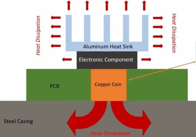
While copper thickness plays a major role in heat spreading, it’s not the only tool for PCB cooling. Thermal vias are another powerful technique to improve heat transfer, especially in multilayer boards. These are small plated holes that connect inner copper layers to outer layers or directly to a heatsink, allowing heat to move vertically through the board.
Thermal vias work by providing a low-resistance path for heat to escape from inner layers to the surface, where it can be dissipated via convection or conduction to a heatsink. For maximum effectiveness, place thermal vias directly under heat-generating components like power transistors or ICs. A typical design might use an array of 0.3 mm diameter vias with a spacing of 1.2 mm, filled with copper to enhance thermal conductivity.
Combining thermal vias with thicker inner copper layers creates a robust thermal management system. The thick copper spreads heat laterally, while the vias transfer it vertically to areas where it can be dissipated. Studies have shown that adding thermal vias can reduce component temperatures by 10-15°C in high-power designs, depending on via density and placement.
Other PCB Cooling Techniques to Consider
Beyond copper thickness and thermal vias, several other PCB cooling strategies can complement your thermal management efforts. Here are a few practical approaches:
- Component Placement: Position high-power components away from each other to avoid concentrated heat zones. Place them near board edges or areas with better airflow for natural convection.
- Heatsinks and Thermal Pads: Attach heatsinks to critical components and use thermal pads to improve heat transfer to the sink. Ensure the PCB layout allows for proper mounting of these cooling aids.
- Board Material Selection: Choose substrates with higher thermal conductivity, such as metal-core PCBs (MCPCBs) for extreme heat applications like LED lighting. Standard FR-4 has a thermal conductivity of only 0.3 W/m·K, while aluminum-backed boards can exceed 2 W/m·K.
- Airflow Optimization: If your device uses forced air cooling (fans), design the PCB layout to align with airflow patterns, ensuring heat is carried away efficiently.
Integrating these techniques with optimized copper thickness ensures a comprehensive approach to PCB thermal management. Each method addresses a different aspect of heat dissipation, creating a balanced design that maximizes performance and reliability.
Practical Tips for Designing with Copper Thickness in Mind
Designing a PCB for optimal heat dissipation requires careful planning. Here are some actionable tips to guide you when considering copper thickness and temperature effects:
- Assess Power Requirements Early: Identify high-power components during the schematic phase and estimate their heat output. Use this data to decide on inner layer copper thickness before layout begins.
- Use Simulation Tools: Leverage thermal simulation software to model heat flow in your PCB. These tools can predict temperature rises based on copper thickness, via placement, and material choices, saving time and reducing costly revisions.
- Balance Cost and Performance: While thicker copper (2-3 oz/ft2) improves inner layer heat dissipation, it raises production costs. Use it only where necessary, such as in power planes near heat sources, and opt for standard thickness (1 oz/ft2) elsewhere.
- Collaborate with Manufacturers: Work closely with your PCB fabrication partner to understand their capabilities and limitations regarding copper thickness and thermal via filling. This ensures your design is manufacturable without unexpected issues.
Challenges and Limitations of Thicker Copper Layers
While thicker copper offers clear benefits for PCB thermal management, it comes with trade-offs. Understanding these challenges helps in making informed design decisions:
- Manufacturing Complexity: Thicker copper requires longer etching times and can lead to undercutting, affecting trace precision. This is a concern for fine-pitch designs with tight tolerances.
- Cost Increase: The cost of a PCB rises with copper thickness due to higher material usage and processing time. For large-scale production, this can impact overall project budgets.
- Weight and Size: Thicker copper adds weight to the board, which may be a concern in portable or weight-sensitive applications like drones or wearables.
- Diminishing Returns: Beyond a certain point, additional copper thickness provides minimal improvement in heat dissipation if other factors (like airflow or heatsink attachment) are the limiting factors.
Designers must weigh these limitations against the thermal benefits to create a cost-effective and efficient PCB design.
Conclusion: Mastering PCB Thermal Management
Effective PCB thermal management is a cornerstone of reliable electronic design, and the role of inner layer heat dissipation cannot be overstated. By carefully selecting the right copper thickness, incorporating thermal vias, and applying complementary PCB cooling techniques, you can significantly reduce temperature rises and extend the lifespan of your devices. The relationship between copper thickness and temperature is a critical factor—thicker copper lowers thermal resistance and spreads heat more effectively, but it must be balanced with cost and manufacturing constraints.
Whether you’re designing for high-power industrial systems or compact consumer electronics, understanding and optimizing copper thickness in inner layers is a secret weapon for tackling heat challenges. With the tips and strategies shared in this guide, you’re well-equipped to create thermally efficient PCB designs that stand up to demanding applications.





