ALLPCB


If you're new to PCB design, understanding PCB trace width is crucial for creating functional and reliable circuit boards. So, what is PCB trace width, and how do you calculate it? Simply put, trace width is the width of the copper paths on a printed circuit board (PCB) that carry electrical signals or power. Calculating the right trace width ensures your board can handle the required current without overheating or failing. For hobby projects or basic designs, you can determine trace width using online calculators or standard guidelines like the IPC-2221, factoring in current, temperature rise, and copper thickness.
In this comprehensive guide, we'll dive deep into everything beginners need to know about PCB trace width. From the basics of why it matters to step-by-step instructions on how to calculate trace width for hobby projects, we've got you covered. Whether you're working on a simple DIY circuit or starting to explore basic PCB design, this tutorial will help you master the essentials of trace width.
What Is PCB Trace Width and Why Does It Matter?
PCB trace width refers to the measurement of the thin copper strips on a circuit board that connect components and carry electrical current. Think of these traces as the "wires" of your PCB. Their width directly affects how much current they can safely handle, how much heat they generate, and how well your circuit performs.
Why is this important for beginners? If a trace is too narrow for the current it carries, it can overheat, leading to damage or even failure of your board. On the other hand, overly wide traces can waste valuable space on your PCB, making your design less efficient. Getting the trace width right ensures safety, reliability, and optimal performance, especially in hobby projects where mistakes can be costly in terms of time and materials.

The Basics of PCB Trace Width in Design
Before diving into calculations, let's cover the fundamental factors that influence trace width in basic PCB design. These include:
- Current Carrying Capacity: The amount of electrical current a trace can handle without overheating. Higher currents require wider traces.
- Temperature Rise: The increase in temperature a trace experiences when current flows through it. You typically want to limit this rise to avoid damage (e.g., a 10°C rise is often a safe target for hobby projects).
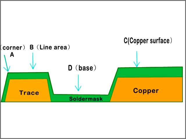
- Copper Thickness: PCB traces are made of copper, and the thickness (measured in ounces per square foot, like 1 oz or 2 oz) affects how much current they can carry. Thicker copper allows for narrower traces at the same current level.
- Trace Location: Traces on the outer layers of a PCB can dissipate heat better than those on inner layers, so inner traces often need to be wider for the same current.
For beginners working on hobby projects, understanding these factors helps in making informed decisions during the design phase. A small LED circuit might only need thin traces, while a power supply board could require much wider ones to handle higher currents.
How to Calculate Trace Width: A Step-by-Step Tutorial
Calculating the correct trace width for your PCB can seem intimidating at first, but it's manageable with the right approach. Here's a simple step-by-step process tailored for beginners:
Step 1: Determine the Current
First, figure out how much current will flow through the trace. For hobby projects, you can often find this information in the datasheet of the components you're using or by calculating it based on your circuit's design. For example, if you're powering a 5V LED strip drawing 500mA (0.5A), that's the current you need to account for.
Step 2: Set a Temperature Rise Limit
Next, decide on an acceptable temperature rise for your trace. A common limit for hobbyists is 10°C above ambient temperature, as it keeps the board safe and prevents excessive heat buildup. For more demanding applications, you might allow a 20°C or 30°C rise, but stick to lower values as a beginner.
Step 3: Check Copper Thickness
Most standard PCBs for hobbyists use 1 oz/ft2 copper, which is about 35 micrometers thick. If you use a different PCB copper thickness (like 2 oz/ft2), note it down, as it impacts the width calculation. Thicker copper can handle more current with a narrower trace.
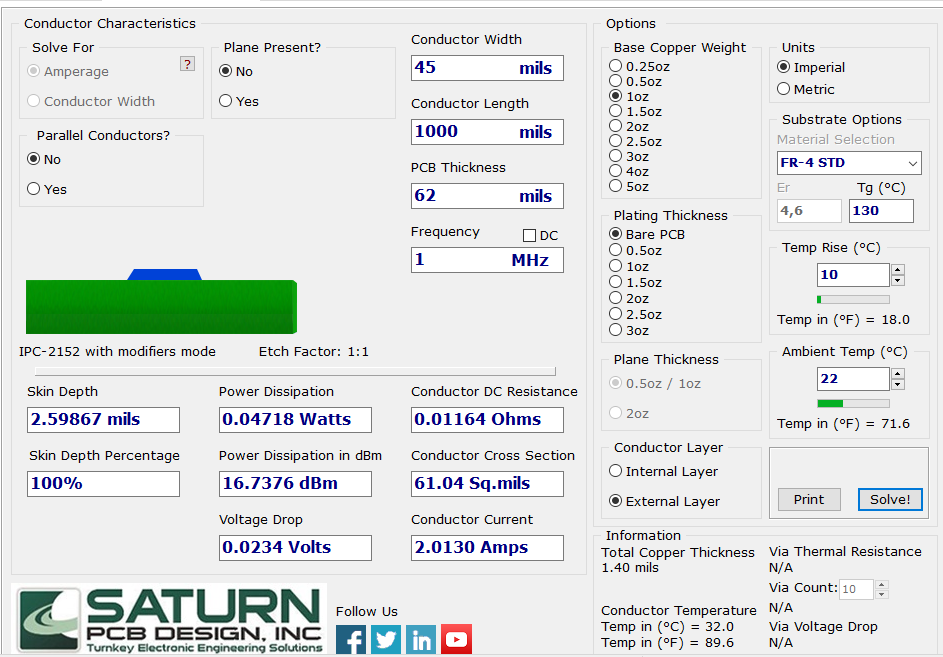
Step 4: Use a Trace Width Calculator or Chart
For beginners, using an online trace width calculator is the easiest way to get accurate results. These tools are based on industry standards like IPC-2221, which provide formulas and data for trace width based on current, temperature rise, and copper thickness. Input your values—current (e.g., 0.5A), temperature rise (e.g., 10°C), and copper thickness (e.g., 1 oz)—and the tool will output the required trace width in mils or millimeters. For instance, a 0.5A current with a 10°C rise on 1 oz copper might require a trace width of around 10 mils (0.254 mm).
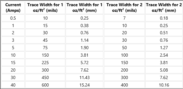
If you prefer a manual approach, you can refer to trace width vs. current tables derived from IPC-2221 standards. These tables show that for 1A on 1 oz copper with a 10°C rise, you’d need a trace width of approximately 20 mils (0.508 mm).
Step 5: Adjust for Inner vs. Outer Layers
If your trace is on an inner layer of a multi-layer PCB, it will need to be wider due to poorer heat dissipation. As a rule of thumb, inner layer traces should be about 1.5 to 2 times wider than outer layer traces for the same current and temperature rise.
Trace Width for Hobby Projects: Practical Tips
When working on hobby projects, you don’t always need to dive into complex calculations. Here are some practical tips to simplify the process while ensuring your PCB performs well:
- Start with Defaults: Many PCB design software tools have default trace widths (often 6-10 mils or 0.15-0.25 mm) that work fine for low-current signals. Use these for non-power traces unless your project demands otherwise.
- Overestimate for Safety: If you’re unsure about the exact current, err on the side of wider traces. For example, if a calculator suggests 15 mils for a trace, consider using 20 mils to give yourself a safety margin.
- Focus on Power Traces: In hobby projects, power traces (those carrying higher currents to supply voltage to components) are where trace width matters most. Signal traces for data or control often carry negligible current and can remain thin.
- Check Manufacturer Limits: Some PCB fabrication services have minimum trace width requirements (e.g., 6 mils). Ensure your design complies with these limits to avoid manufacturing issues.
For a practical example, imagine you're designing a PCB for a small robot with a motor driver drawing 2A. Using a trace width calculator, you find that for a 10°C temperature rise on 1 oz copper, you need a trace width of about 40 mils (1.016 mm). By rounding up to 50 mils, you add extra safety and ensure your board can handle the load without overheating.
Common Mistakes to Avoid in PCB Trace Width Design
As a beginner, it’s easy to make mistakes when determining trace width. Here are some pitfalls to watch out for:
- Underestimating Current: Always double-check the maximum current your circuit might draw, including spikes or inrush currents, to avoid designing traces that are too narrow.
- Ignoring Temperature Rise: Not accounting for heat buildup can lead to traces that burn out over time. Stick to conservative temperature rise limits like 10°C or 20°C.
- Forgetting Layer Differences: If your design has inner layers, remember that traces there need to be wider due to reduced heat dissipation.
- Overcomplicating Low-Power Designs: For simple hobby projects with low currents (under 100mA), you often don’t need to overthink trace width. Default settings in design software are usually sufficient.
Advanced Considerations for Trace Width in Basic PCB Design
While beginners can often stick to basic calculations, it’s worth understanding a few advanced factors that might come into play as you gain experience:
- Impedance Control: For high-speed signals (like USB or HDMI), trace width affects impedance, which must match the circuit's requirements (e.g., 50 ohms for many RF applications). This is less relevant for most hobby projects but critical in advanced designs.
- Signal Integrity: Narrow traces can introduce resistance and affect signal quality in high-frequency circuits. Wider traces or specific routing techniques might be needed to maintain performance
Suggested Reading: Decoding PCB Trace Width: A Signal Integrity Deep Dive
- Thermal Management: In high-current applications, wider traces or additional copper pours can help dissipate heat more effectively, reducing the risk of hotspots.
For now, as a beginner, focus on getting the current-carrying capacity right. As you grow more comfortable with PCB design, you can explore these advanced topics to refine your skills.
Tools and Resources for Calculating Trace Width
Fortunately, you don’t need to do complex math to determine trace width. Here are some tools and resources that can make the process easier for hobbyists and beginners:
- Online Calculators: The PCB trace width calculator allows you to input current, temperature rise, and copper thickness to get an instant trace width value. It is often based on industry standards and are highly reliable for basic designs.
- PCB Design Software: Most design software includes built-in calculators or rules that automatically suggest or enforce trace widths based on your circuit’s requirements.
- Reference Charts: Industry-standard charts based on IPC-2221 provide trace width values for different currents and temperature rises. These are great for quick lookups without software.
Using these tools, you can confidently design PCBs that meet your project’s needs without second-guessing your calculations.
Conclusion: Mastering PCB Trace Width for Your Projects
Understanding and calculating PCB trace width is a fundamental skill for anyone stepping into the world of circuit board design. By following the steps outlined in this PCB trace width tutorial, you can ensure your designs are safe, efficient, and reliable—even as a beginner. Whether you're working on hobby projects or diving into basic PCB design, remember to prioritize current capacity, limit temperature rise, and use available tools to simplify the process.
Start small with your trace width calculations, use conservative estimates for safety, and don’t hesitate to leverage online calculators or software features to guide you. As you gain experience, you’ll develop a better intuition for balancing trace width with other design constraints, setting the foundation for more complex projects in the future.
With this guide, you’re well on your way to mastering how to calculate trace width and applying it effectively in your designs. Keep experimenting, learning, and refining your skills, and you’ll soon create PCBs that perform flawlessly every time.