 ALLPCB


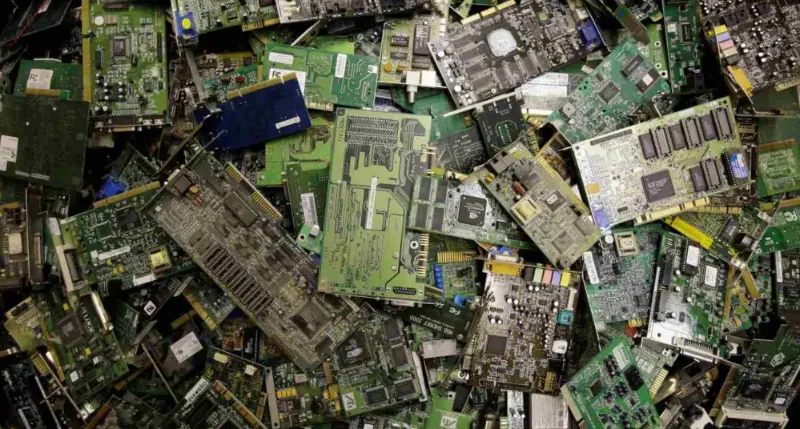
In today’s fast-paced world of technology, electronic devices are constantly being upgraded, leading to a growing pile of electronic waste (e-waste). A key part of managing this waste lies in reverse logistics for electronics PCBs (Printed Circuit Boards). But what exactly is reverse logistics, and how does it contribute to sustainable PCB disposal? Simply put, reverse logistics involves the process of handling end-of-life electronics by returning them through the supply chain for recycling, refurbishment, or proper disposal. When applied to PCBs, it offers a sustainable approach to reduce environmental harm and recover valuable materials.
In this blog, we’ll dive deep into the importance of reverse logistics strategies for electronics, the PCB recycling process, and effective e-waste management for PCBs. Whether you’re an engineer, a manufacturer, or simply someone interested in sustainable practices, this guide will provide actionable insights into making electronics disposal more eco-friendly.
What is Reverse Logistics for Electronics PCBs?
Reverse logistics refers to the process of moving goods from their final destination back through the supply chain for purposes like recycling, refurbishing, or disposal. In the context of electronics PCBs, it means collecting used or obsolete circuit boards from consumers or businesses and ensuring they are processed in an environmentally responsible way. Unlike traditional logistics, which focuses on delivering products to customers, reverse logistics deals with the “return” journey of these products.
For PCBs, which are the backbone of nearly every electronic device, reverse logistics plays a critical role in addressing e-waste. These boards often contain hazardous materials like lead and mercury, as well as valuable metals like gold and copper. A well-structured reverse logistics system helps prevent toxic substances from ending up in landfills while recovering resources for reuse.
Why Reverse Logistics Matters for Sustainable PCB Disposal
The global e-waste crisis is staggering. According to recent studies, over 50 million metric tons of e-waste are generated annually, with only about 20% being properly recycled. PCBs, as core components of electronics, contribute significantly to this waste. Without proper handling, the hazardous materials in PCBs can leak into soil and water, posing serious health and environmental risks.
Reverse logistics offers a solution by creating a structured pathway for sustainable PCB disposal. It ensures that end-of-life electronics are collected, dismantled, and recycled rather than discarded. This not only reduces pollution but also conserves natural resources by recovering materials that can be reused in manufacturing. For instance, recycling just one ton of PCBs can recover up to 800 grams of gold and several kilograms of copper, reducing the need for mining new materials.
Key Reverse Logistics Strategies for Electronics
Implementing effective reverse logistics strategies for electronics requires careful planning and coordination. Below are some proven approaches to manage PCBs sustainably:
1. Establishing Collection Networks
The first step in reverse logistics is collecting used electronics from consumers and businesses. Setting up convenient drop-off points, partnering with retailers for take-back programs, and offering mail-back services are effective ways to gather e-waste. For example, collection centers can be placed in urban areas where electronic usage is high, making it easy for people to return old devices.
2. Partnering with Certified Recyclers
Once collected, PCBs must be sent to certified recycling facilities that follow strict environmental standards. These facilities use specialized equipment to safely extract hazardous materials and recover valuable metals. Partnering with trusted recyclers ensures compliance with regulations and minimizes the risk of improper disposal.
3. Implementing Tracking Systems
Using technology to track e-waste throughout the reverse logistics process is crucial for transparency. Barcode systems or digital platforms can monitor the journey of PCBs from collection to final processing, ensuring nothing is lost or mishandled. This also helps in generating reports for regulatory compliance.
4. Educating Consumers and Businesses
Awareness is key to the success of reverse logistics. Many people are unaware of the importance of recycling electronics or where to dispose of them. Companies can play a role by providing information on sustainable PCB disposal through websites, product manuals, or community outreach programs.
The PCB Recycling Process: Step by Step
Understanding the PCB recycling process is essential for anyone involved in electronics manufacturing or disposal. This process not only reduces environmental impact but also recovers valuable materials for reuse. Here’s how it works:
Step 1: Collection and Sorting
The process begins with collecting used electronics and sorting them to separate PCBs from other components. This can be done manually or with automated systems, depending on the volume of waste. Sorting ensures that only PCBs move to the next stage, while other materials like plastics and batteries are handled separately.
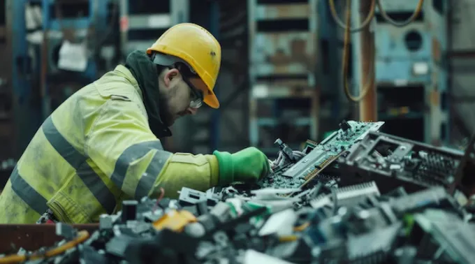
Step 2: Dismantling and Component Removal
Once sorted, PCBs are dismantled to remove individual components like capacitors, resistors, and chips. This step is often done manually to avoid damaging reusable parts. Components that can be refurbished are set aside, while the bare boards move to the next phase.
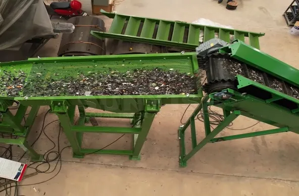
Step 3: Shredding and Grinding
The bare PCBs are shredded into small pieces using industrial shredders. This breaks down the boards into a mix of metals, plastics, and other materials. Grinding further reduces the size of particles, making it easier to separate different materials in the next step.
Step 4: Material Separation
Specialized equipment like magnetic separators, air classifiers, and eddy current separators are used to divide the shredded material into metals (like copper and aluminum) and non-metals (like fiberglass and epoxy resin). This step is critical for maximizing material recovery.
Step 5: Refining and Recovery
Recovered metals are sent for refining to remove impurities, making them suitable for reuse in manufacturing. For instance, copper from PCBs can be melted down and turned into new wires or circuit board traces. Hazardous materials, if present, are treated and disposed of according to environmental regulations.
E-Waste Management for PCBs: Challenges and Solutions
While reverse logistics and recycling offer promising solutions, e-waste management for PCBs comes with its own set of challenges. Let’s explore these issues and how they can be addressed.
Challenge 1: Low Recycling Rates
Despite growing awareness, a significant portion of e-waste still ends up in landfills. Many regions lack the infrastructure for proper collection and recycling, leading to illegal dumping or informal processing that harms the environment.
Solution: Governments and industries can work together to build more recycling facilities and establish stricter regulations on e-waste disposal. Incentives like tax breaks for recycling programs can also encourage participation.
Challenge 2: Hazardous Materials
PCBs often contain toxic substances like lead, cadmium, and brominated flame retardants. If not handled properly during recycling, these materials can cause severe environmental and health problems.
Solution: Investing in advanced recycling technologies that safely extract and neutralize hazardous materials is essential. Training workers on proper handling techniques also reduces risks.
Challenge 3: High Costs of Reverse Logistics
Setting up collection networks, transporting e-waste, and operating recycling facilities can be expensive, especially for small businesses or developing regions.
Solution: Collaboration between manufacturers, governments, and recycling firms can help share costs. Extended Producer Responsibility (EPR) policies, where manufacturers are responsible for the end-of-life management of their products, can also drive funding for reverse logistics.
Benefits of Sustainable PCB Disposal Through Reverse Logistics
Adopting reverse logistics for sustainable PCB disposal offers numerous benefits, both for the environment and the economy. Here are some key advantages:
- Environmental Protection: Proper recycling prevents toxic materials from contaminating soil and water, reducing pollution and protecting ecosystems.
- Resource Conservation: Recovering metals and other materials from PCBs reduces the need for mining, saving natural resources and energy. For example, recycling copper from PCBs uses up to 85% less energy than extracting it from ore.
- Economic Opportunities: The recycling industry creates jobs in collection, processing, and refining, contributing to local economies.
- Regulatory Compliance: Following sustainable practices helps companies meet environmental regulations and avoid penalties.
How Manufacturers Can Support Reverse Logistics for PCBs
Manufacturers play a pivotal role in making reverse logistics effective. By integrating sustainable practices into their operations, they can significantly reduce the environmental impact of PCBs. Here are some ways they can contribute:
- Design for Recycling: Create PCBs with materials that are easier to recycle and components that can be easily disassembled. For instance, using fewer hazardous substances can simplify the recycling process.
- Take-Back Programs: Offer programs where customers can return old electronics directly to the manufacturer for recycling.
- Collaboration: Work with recycling partners to ensure end-of-life products are handled responsibly.
- Transparency: Provide clear information on how products can be disposed of or recycled, helping customers make informed decisions.
Future Trends in Reverse Logistics and PCB Recycling
As technology advances, so do the methods for managing e-waste. Here are some emerging trends in reverse logistics and the PCB recycling process:
- Automation in Recycling: Robotics and AI are being used to automate sorting and dismantling, increasing efficiency and reducing costs.
- Circular Economy Models: More companies are adopting circular economy principles, focusing on reusing and recycling materials to create a closed-loop system.
- Stricter Regulations: Governments worldwide are implementing tougher e-waste laws, pushing industries to prioritize sustainable practices.
- Advanced Recovery Techniques: New methods, such as chemical leaching and bioleaching, are being developed to extract rare metals from PCBs more effectively.
Conclusion: Building a Sustainable Future with Reverse Logistics
Reverse logistics for electronics PCBs offers a powerful solution to the growing e-waste crisis. By implementing effective reverse logistics strategies for electronics, understanding the PCB recycling process, and prioritizing e-waste management for PCBs, we can achieve sustainable PCB disposal that benefits both the environment and the economy. From collection to material recovery, every step in the process plays a vital role in reducing waste and conserving resources.
As technology continues to evolve, staying committed to sustainable practices is more important than ever. Whether you’re a manufacturer, engineer, or consumer, you have a role to play in supporting reverse logistics and ensuring a greener future for the electronics industry. Let’s work together to turn e-waste into an opportunity for innovation and sustainability.


