ALLPCB


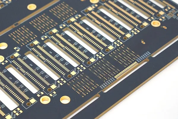
In the fast-evolving world of electronics, precision in PCB (Printed Circuit Board) manufacturing is more important than ever. One critical technique that stands out for ensuring high performance in high-speed designs is controlled depth drilling. But what exactly is controlled depth drilling, and how does it help with PCB via stub removal? Simply put, it’s a method used to drill vias to a specific depth, removing unused portions (stubs) that can interfere with signal integrity. This process, often called back drilling, is essential for optimizing signal performance in multilayer boards.
In this comprehensive guide, we’ll dive deep into the art of controlled depth drilling, exploring its importance for precision drilling of PCB vias, the equipment used, comparisons like back drilling vs blind vias, and how it ties into PCB signal integrity optimization. Whether you’re an engineer or a designer, this blog will provide actionable insights to enhance your understanding and application of these techniques.
What Is Controlled Depth Drilling and Why Does It Matter?
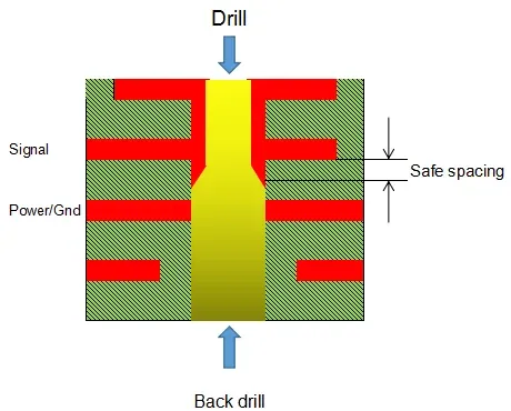
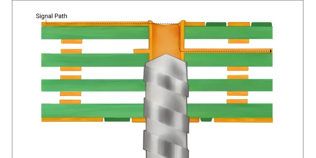
Controlled depth drilling is a specialized manufacturing process used in PCB production to drill vias to a precise depth rather than through the entire board. This technique is often referred to as back drilling when it’s used to remove via stubs—unused portions of a via that extend beyond the signal layer. These stubs can cause signal reflections, leading to data loss or interference in high-speed circuits operating at frequencies above 1 GHz.
Why does this matter? In high-speed designs, even a small stub measuring 0.010 inches can create significant impedance mismatches, causing signal degradation. By removing these stubs through controlled depth drilling, manufacturers can minimize signal loss and electromagnetic interference (EMI), ensuring cleaner and faster data transmission. This is especially critical in applications like telecommunications, aerospace, and data centers, where signal integrity is non-negotiable.
The Science Behind PCB Drilling Depth Control
Achieving precision in PCB drilling depth control requires a deep understanding of both the materials and the equipment involved. Multilayer PCBs are made of alternating layers of conductive copper and insulating materials like FR-4, which can vary in thickness and hardness. Drilling too deep or not deep enough can damage the board or leave residual stubs, both of which compromise performance.
Modern PCB drilling depth control relies on advanced machinery equipped with sensors and software to monitor drilling depth in real-time. These systems can achieve tolerances as tight as ±0.002 inches, ensuring that the drill stops exactly at the target layer. For example, in a 12-layer board, the drill might need to stop just 0.020 inches from the surface to avoid damaging an internal signal layer while removing the stub.
The process starts with a detailed design file that specifies the exact depth for each via. During drilling, the equipment uses feedback mechanisms to adjust for variables like drill bit wear or material inconsistencies, maintaining precision across thousands of vias on a single board.
Precision Drilling for PCB Vias: Challenges and Solutions
Precision drilling of PCB vias is no small feat. Vias are tiny—often less than 0.010 inches in diameter—and must be drilled with extreme accuracy to avoid misalignment or damage. One major challenge is drill bit wander, where the bit deviates from its intended path due to material inconsistencies or excessive speed. This can result in vias that are off-center, impacting connectivity and signal performance.
To overcome this, manufacturers use high-speed spindles operating at up to 200,000 RPM, paired with rigid machine frames to minimize vibration. Additionally, advanced controlled depth drilling equipment often includes laser-guided alignment systems to ensure the drill hits the exact spot every time. Cooling systems are also critical to prevent overheating, which can cause delamination of the PCB layers.
Another challenge is managing the depth itself. If the drill goes too far, it risks damaging internal layers; if it stops too soon, a stub remains, affecting signal integrity. The solution lies in real-time depth monitoring and automated adjustments, ensuring consistent results even across large production runs.
Controlled Depth Drilling Equipment: Tools of the Trade
The heart of controlled depth drilling lies in the equipment used. Today’s advanced machinery is designed to handle the demands of high-speed, high-precision PCB manufacturing. Here are some key features of controlled depth drilling equipment:
- High-Speed Spindles: Capable of rotating at speeds exceeding 150,000 RPM, these spindles ensure clean, accurate holes with minimal burrs.
- Depth Sensors: Integrated sensors provide real-time feedback on drill depth, allowing for adjustments on the fly with tolerances as low as ±0.001 inches.
- Automated Tool Changers: These systems switch between different drill bit sizes automatically, optimizing efficiency for boards with varying via sizes.
- Laser Alignment: Laser systems guide the drill to the exact coordinates, reducing errors in via placement.
Investing in such equipment is crucial for manufacturers aiming to produce high-quality boards for high-speed applications. While the upfront cost can be significant, the reduction in signal issues and rework makes it a worthwhile investment.
Back Drilling vs Blind Vias: Which Is Right for Your Design?
When it comes to managing via stubs and optimizing signal performance, two techniques often come into play: back drilling (a form of controlled depth drilling) and blind vias. Both have their place in PCB design, but they serve different purposes and come with unique advantages and challenges.
Back Drilling: As discussed, back drilling involves drilling from the opposite side of the board to remove via stubs after the initial through-hole via is created. It’s ideal for multilayer boards where cost efficiency is a priority, as it uses standard through-hole technology before applying precision drilling. However, it requires additional manufacturing steps, increasing production time.
Blind Vias: Blind vias, on the other hand, are drilled only partway through the board during the initial manufacturing process, connecting an outer layer to an inner layer without creating a stub. This eliminates the need for a secondary drilling step, saving time. However, blind vias are more complex to design and manufacture, often increasing the cost of the PCB.
Choosing between the two depends on your project’s needs. For high-speed designs with tight budgets, back drilling offers a cost-effective way to achieve PCB signal integrity optimization. For compact designs where space and layer transitions are critical, blind vias might be the better choice despite the higher cost.
PCB Signal Integrity Optimization Through Via Stub Removal
Signal integrity is the cornerstone of high-speed PCB performance. As data rates climb—often exceeding 10 Gbps in modern designs—any impedance mismatch or signal reflection can lead to errors or data loss. Via stubs are a major culprit, acting as tiny antennas that reflect signals back along the trace, causing interference.
By using controlled depth drilling to remove these stubs, designers can achieve PCB signal integrity optimization. For instance, removing a stub can reduce signal reflection by up to 50%, lowering the bit error rate (BER) in high-speed digital circuits. This is especially important in applications like 5G infrastructure, where signal clarity directly impacts performance.
Beyond stub removal, other factors like trace length matching and proper grounding also play a role in signal integrity. However, eliminating via stubs through precision drilling is often the first and most impactful step. When combined with simulation tools to predict signal behavior, controlled depth drilling ensures that your PCB performs reliably under real-world conditions.
Best Practices for Implementing Controlled Depth Drilling
To get the most out of controlled depth drilling, follow these best practices during design and manufacturing:
- Accurate Design Files: Ensure your PCB design software specifies exact drilling depths for each via. Include clear notes on which layers need stub removal to avoid errors.
- Material Selection: Choose PCB materials with consistent thickness and dielectric properties to minimize drilling variations. Standard FR-4 is often sufficient for most designs, but high-frequency applications may require advanced laminates.
- Collaborate with Manufacturers: Work closely with your manufacturing partner to confirm their equipment capabilities and tolerances for controlled depth drilling. This ensures your design is feasible for production.
- Testing and Validation: After manufacturing, use time-domain reflectometry (TDR) to verify that stubs have been effectively removed and impedance matches the design specs (e.g., 50 ohms for most high-speed signals).
By following these steps, you can reduce manufacturing defects and achieve consistent results, even in complex multilayer designs.
The Future of Controlled Depth Drilling in PCB Manufacturing
As electronic devices continue to shrink and data rates soar, the demand for precision in PCB manufacturing will only grow. Controlled depth drilling is poised to evolve with advancements in automation and machine learning. Future equipment may use AI to predict and adjust for material variations in real-time, pushing tolerances even tighter than today’s ±0.001 inches.
Additionally, the rise of 5G, IoT, and autonomous systems will drive the need for even more sophisticated signal integrity solutions. Techniques like controlled depth drilling will remain at the forefront, ensuring that PCBs can handle the challenges of tomorrow’s technologies.
Conclusion: Mastering Precision for High-Performance PCBs
Controlled depth drilling is truly an art form in the world of PCB manufacturing. By mastering PCB drilling depth control and precision drilling of PCB vias, manufacturers can eliminate via stubs and achieve unparalleled PCB signal integrity optimization. Whether you’re weighing back drilling vs blind vias or investing in advanced controlled depth drilling equipment, understanding this process is key to staying competitive in high-speed design.
At ALLPCB, we’re committed to helping engineers and designers navigate these complex challenges with cutting-edge manufacturing solutions. By leveraging the power of controlled depth drilling, you can ensure your PCBs deliver the performance and reliability your applications demand. Let’s build the future of electronics together, one precise via at a time.