ALLPCB


Designing a printed circuit board (PCB) for an e-reader, especially one with an E-Ink display, requires careful attention to detail. Electromagnetic interference (EMI) can disrupt the performance of these devices, leading to display glitches or reduced signal clarity. In this ultimate guide, we’ll explore how to create an effective PCB layout for e-readers, focusing on E-Reader PCB EMI reduction, signal integrity PCB design, PCB layout for E-Ink, noise reduction PCB techniques, and grounding techniques PCB. Whether you're an engineer or a designer, this blog will provide actionable tips to ensure your e-reader delivers a crystal-clear display.
Why EMI Matters in E-Reader PCB Design
EMI is unwanted electromagnetic energy that can interfere with the signals in your e-reader’s PCB. For devices using E-Ink displays, which are known for low power consumption and high readability, even small amounts of interference can cause flickering, ghosting, or slow refresh rates. Reducing EMI is critical to maintaining signal integrity and ensuring the display functions smoothly.
E-Ink displays operate with low-frequency signals, typically in the range of 1 to 10 MHz for refresh rates. However, nearby high-frequency components, like Wi-Fi modules or power regulators operating at 100 MHz or more, can introduce noise. This noise can couple into sensitive traces, disrupting the delicate balance needed for a clear display. Let’s dive into the key strategies for minimizing EMI and optimizing your PCB layout for e-readers.
Key Principles of E-Reader PCB Layout for EMI Reduction
Creating a PCB layout that minimizes EMI starts with understanding the unique needs of e-readers. Below are the core principles to follow for E-Reader PCB EMI reduction and a high-quality display.
1. Optimize Component Placement for Noise Reduction
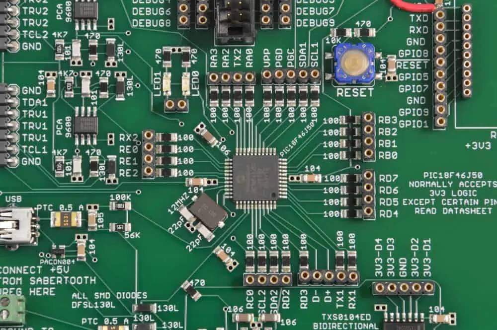
The placement of components on your PCB plays a big role in controlling EMI. High-frequency components, such as switching regulators or wireless modules, should be placed far from sensitive areas like the E-Ink display driver circuits. For instance, keep power management ICs at least 20-30 mm away from the display controller to avoid noise coupling.
Group similar components together. Place analog components near each other and digital components in a separate area. This reduces the chances of crosstalk between different signal types. Also, position decoupling capacitors as close as possible to the power pins of ICs—ideally within 1-2 mm—to filter out high-frequency noise.
2. Prioritize Signal Integrity in PCB Design
Signal integrity PCB design is about ensuring that signals travel through the board without distortion or loss. For E-Ink displays, signal integrity is crucial because even small timing errors can cause display artifacts. Start by keeping signal traces short and direct. Long traces act like antennas, picking up or radiating EMI.
For critical signals, such as those between the display controller and the E-Ink panel, maintain a controlled impedance. A common target for these traces is 50 ohms, which helps match the impedance of the driver and display. Use a trace width calculator to achieve this value based on your board’s dielectric constant (often around 4.5 for FR-4 material) and layer stack-up.
Additionally, avoid sharp corners in trace routing. Use 45-degree angles or curves to minimize signal reflections, which can introduce noise. If your design includes high-speed signals, consider using differential pairs for better noise immunity.
3. Implement Effective Grounding Techniques for PCB
Grounding techniques PCB are at the heart of EMI control. A solid ground plane is essential for providing a low-impedance return path for signals and reducing noise. For e-reader PCBs, use a continuous ground plane on one layer of the board, ideally directly beneath the signal layer. Avoid splitting the ground plane unless absolutely necessary, as splits can create loops that radiate EMI.
For multi-layer boards (common in e-readers with 4 or more layers), dedicate one layer entirely to ground. Connect all ground pins of components to this plane using vias placed close to the pins—within 0.5 mm if possible. This minimizes inductance and keeps noise levels low. If your design includes both analog and digital sections, consider using separate ground planes connected at a single point to prevent noise from one section affecting the other.
Advanced Strategies for Noise Reduction in PCB Design
Beyond the basics, there are advanced techniques for noise reduction PCB design that can further enhance the performance of your e-reader. These strategies target specific sources of EMI and ensure a cleaner signal environment.
4. Use EMI Filters and Ferrite Beads
Power lines are a common entry point for EMI in e-reader designs. To combat this, add EMI filters or ferrite beads on the power supply lines feeding the display controller and other sensitive circuits. A ferrite bead with a current rating of 500 mA and an impedance of 600 ohms at 100 MHz can effectively block high-frequency noise while allowing DC power to pass through.
Place these components as close as possible to the power entry point of the IC. Pair them with a bypass capacitor (e.g., 0.1 μF) to create a low-pass filter that further reduces noise. This combination can cut down high-frequency interference by up to 40 dB, significantly improving display clarity.
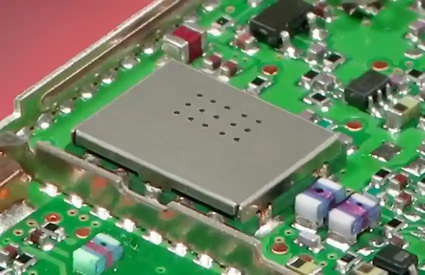
5. Shield Sensitive Areas
For e-readers with integrated wireless modules (like Wi-Fi or Bluetooth), shielding is a must. Use metal shields or cans over high-frequency components to contain their electromagnetic radiation. Alternatively, apply a shielding layer in the PCB stack-up by placing a ground plane above or below noisy areas.
If shielding hardware isn’t an option, create a “guard ring” around sensitive components using ground vias spaced every 5-10 mm. This ring acts as a barrier, absorbing stray EMI before it reaches critical circuits like the E-Ink driver.
6. Minimize Loop Areas in Power and Signal Paths
Large loop areas in power or signal paths can act as antennas, radiating or picking up EMI. To avoid this, route power and ground traces close together to keep the loop area small. For example, when routing power to the display driver, place the return path (ground trace or plane) directly beneath the power trace on an adjacent layer. This reduces inductance and cuts down on radiated noise.
For signal traces, avoid creating loops by routing them over a continuous ground plane. If a trace must cross a split in the ground plane, add a stitching capacitor (e.g., 0.01 μF) near the crossing to provide a return path for high-frequency signals.
Special Considerations for PCB Layout with E-Ink Displays
The unique nature of E-Ink technology demands specific attention in PCB layout for E-Ink. These displays are highly sensitive to noise and require precise voltage levels for operation. Let’s explore tailored approaches to ensure optimal performance.
7. Manage Power Supply Stability for E-Ink
E-Ink displays often require multiple voltage levels, such as +15V, -15V, and +22V, for driving the display particles. Any ripple or noise in these voltages can cause uneven pixel updates or ghosting. Use low-dropout (LDO) regulators with a ripple rejection ratio of at least 60 dB to provide clean power to the display driver.
Additionally, place bulk capacitors (e.g., 10 μF) near the power input of the display module to stabilize the supply during sudden current draws. Combine these with smaller ceramic capacitors (e.g., 0.1 μF) to handle high-frequency noise.
8. Route Display Signals with Care
The data and control signals for E-Ink displays, such as source and gate lines, are particularly vulnerable to interference. Route these traces on inner layers of the PCB if possible, sandwiching them between ground planes to shield against external noise. Keep trace lengths under 50 mm to minimize delay and signal degradation.
If routing on outer layers is unavoidable, avoid running these traces parallel to high-frequency lines (like clock signals) for more than 10 mm. Crosstalk can introduce errors in display updates, leading to visible artifacts.
Testing and Validation for EMI-Free Performance
Once your PCB layout is complete, testing is essential to confirm that EMI is under control. Use an oscilloscope to measure noise levels on power lines and signal traces. Look for spikes or ripples exceeding 50 mV, as these can affect E-Ink display performance. If noise is detected, revisit your decoupling and grounding strategies.
For comprehensive EMI testing, consider using a spectrum analyzer to identify radiated emissions in the frequency range of 30 MHz to 1 GHz. Compare your results against regulatory standards like FCC Part 15 or CISPR 22 to ensure compliance. If emissions are high, add additional shielding or adjust component placement.
Conclusion: Building Better E-Reader PCBs with EMI in Mind
Designing a PCB for an e-reader with an E-Ink display is a balancing act. By focusing on E-Reader PCB EMI reduction, signal integrity PCB design, and tailored PCB layout for E-Ink, you can create a device that delivers a crystal-clear display free from interference. Implementing robust noise reduction PCB techniques and effective grounding techniques PCB will ensure your design performs reliably in real-world conditions.
Start with careful component placement, prioritize signal integrity, and use advanced shielding and filtering methods to keep EMI at bay. With these strategies, your e-reader PCB will not only meet performance expectations but also stand out for its quality and reliability. Let’s build smarter, quieter, and more efficient designs together!