ALLPCB


If you're looking for insights on using heavy copper PCBs in base stations, you've come to the right place. Heavy copper PCBs, also known as high current or thick copper PCBs, are critical for power distribution in base stations due to their ability to handle high currents and improve thermal management. In this blog, we'll dive deep into the design and manufacturing considerations for these specialized boards, ensuring optimal performance in demanding telecom applications.
Base stations, the backbone of modern communication networks, require robust power systems to support high data traffic and continuous operation. Heavy copper PCBs play a vital role in meeting these demands. Let’s explore why they are essential, how to design them effectively, and the key factors to consider during manufacturing.
What Are Heavy Copper PCBs and Why Are They Essential for Base Stations?
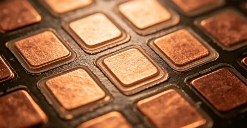
Heavy copper PCBs are printed circuit boards with copper thicknesses exceeding 3 ounces per square foot (oz/ft2), or approximately 4 mils (100 microns). Unlike standard PCBs with 1-2 oz/ft2 copper, these boards are built to carry high currents and dissipate heat efficiently, making them ideal for power-intensive applications like base station power PCBs.
In base stations, which power cellular networks and handle significant electrical loads, heavy copper PCBs are often used in power distribution systems. They ensure stable voltage delivery to critical components, reduce energy losses, and withstand the thermal stress of continuous operation. Their ability to manage currents as high as 20-30 amperes per trace (depending on width and thickness) makes them indispensable for high current PCB designs in telecom infrastructure.
Key Benefits of Heavy Copper PCBs in Base Station Applications
Understanding the advantages of thick copper PCBs helps highlight their importance in base station power systems. Here are the primary benefits:
- High Current Carrying Capacity: With copper thicknesses ranging from 3 oz/ft2 to 10 oz/ft2 or more, these PCBs can handle currents far exceeding standard boards, often supporting loads of 50 amperes or higher with proper trace design.
- Improved Thermal Management: Heavy copper dissipates heat effectively, reducing hotspot formation in base station power PCBs operating under continuous high loads. This can lower operating temperatures by 10-20°C compared to standard copper boards under similar conditions.
- Enhanced Durability: Thicker copper layers withstand repeated thermal cycles, ensuring reliability in harsh environments where base stations are often exposed to temperature fluctuations.
- Reduced Voltage Drop: Thicker traces lower resistance, minimizing voltage drops across long distances in power distribution PCBs, which is critical for maintaining signal integrity in base stations.
Design Considerations for Heavy Copper PCBs in Base Stations
Designing a heavy copper PCB for base station applications requires careful planning to balance performance, cost, and manufacturability. Below are the key factors to keep in mind:
1. Copper Thickness Selection
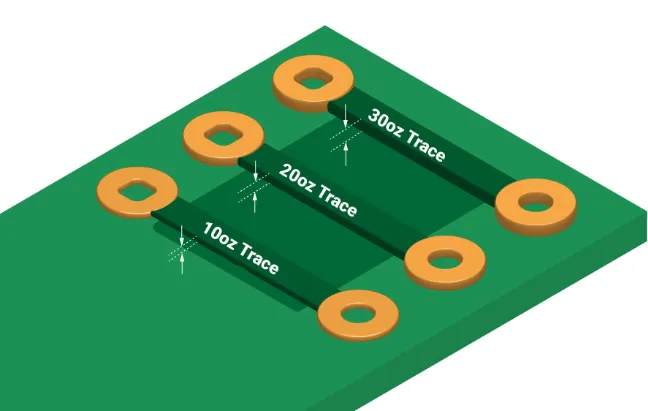
Choosing the right copper thickness is the foundation of high current PCB design. For base stations, copper weights of 4-6 oz/ft2 are common for outer layers, while inner layers might use 3-4 oz/ft2. The thickness directly impacts current capacity; for instance, a 1-inch-wide trace with 4 oz/ft2 copper can carry around 20 amperes safely at room temperature, while 6 oz/ft2 can handle closer to 30 amperes.
However, thicker copper increases board weight and cost, so it’s essential to calculate the minimum thickness needed based on current requirements and thermal constraints using tools like current-carrying capacity charts or simulation software.
2. Trace Width and Spacing
Wider traces are necessary to handle high currents without overheating. A general rule of thumb is to increase trace width by 0.5 mm for every 10 amperes of current. For a 20-ampere load on a 4 oz/ft2 copper layer, a trace width of 2-3 mm is often sufficient, assuming a temperature rise of no more than 10°C.
Spacing between traces must also account for high voltages in base station power PCBs to prevent arcing. A minimum clearance of 0.5 mm for every 100 volts is a good starting point, though specific standards like IPC-2221 may dictate stricter rules based on the operating environment.
3. Thermal Management Design
Base stations often operate in outdoor or confined spaces with limited airflow, making thermal management critical. Heavy copper PCBs naturally aid heat dissipation, but additional design features can enhance performance:
- Thermal Vias: Adding vias under high-power components can transfer heat to other layers or heat sinks, reducing surface temperatures by up to 15% in some designs.
- Copper Planes: Large copper areas or dedicated ground planes act as heat spreaders, distributing thermal energy across the board.
- Component Placement: Position high-power components away from each other to avoid concentrated heat buildup.
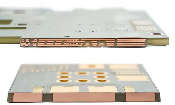
4. Layer Stack-Up for Power Distribution
In power distribution PCBs for base stations, a multilayer design is often necessary to separate power and signal layers. Heavy copper can be used on power layers (inner or outer) to handle high currents, while thinner copper (1-2 oz/ft2) suffices for signal layers. A typical 4-layer stack-up might include:
- Top Layer: Signal and low-power traces (1 oz/ft2)
- Inner Layer 1: Power distribution (4 oz/ft2)
- Inner Layer 2: Ground plane (4 oz/ft2)
- Bottom Layer: Signal and control circuits (1 oz/ft2)
This configuration minimizes interference between power and signal paths while optimizing current flow.
5. Compliance with Standards
Base station designs must adhere to industry standards like IPC-2152 for current-carrying capacity and IPC-6012 for PCB qualification. These standards ensure that heavy copper PCBs meet reliability and safety requirements under high current and thermal stress conditions.
Manufacturing Considerations for Heavy Copper PCBs
Manufacturing thick copper PCBs presents unique challenges due to the material’s properties and the precision required for high current applications. Here are the critical aspects to consider during production:
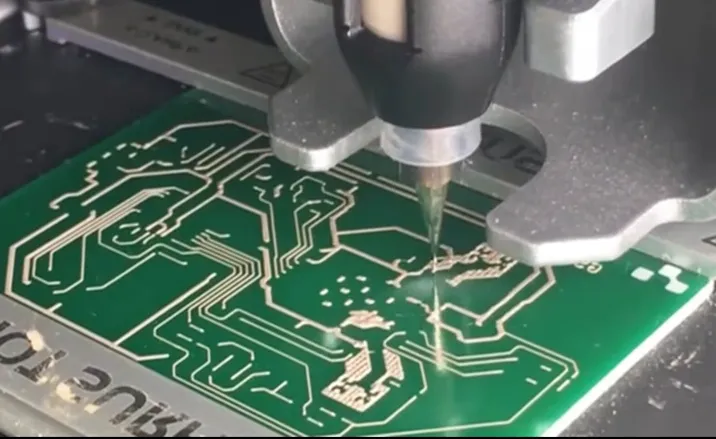
1. Etching Challenges with Thick Copper
Etching heavy copper layers is more difficult than standard copper due to the increased thickness. Over-etching can lead to undercuts, reducing trace width and current capacity, while under-etching leaves copper residue, risking short circuits. Advanced etching techniques, such as differential etching, are often used to achieve precise trace geometries. Manufacturers must maintain tight tolerances, typically within ±10% of the designed trace width, to ensure performance.
2. Lamination and Material Selection
Heavy copper PCBs require robust substrate materials to handle thermal expansion and mechanical stress. High-Tg FR-4 or polyimide materials are preferred for base station applications, as they offer glass transition temperatures above 170°C, ensuring stability under high heat. During lamination, uniform pressure and temperature control are critical to prevent delamination, especially in multilayer boards with varying copper thicknesses.
3. Plating and Surface Finish
For high current PCBs, through-hole plating must be thick and uniform to ensure reliable connections between layers. A minimum plating thickness of 1.5 mils (38 microns) is often recommended for vias carrying high currents. Surface finishes like ENIG (Electroless Nickel Immersion Gold) or HASL (Hot Air Solder Leveling) are suitable for heavy copper boards, providing corrosion resistance and solderability without compromising conductivity.
4. Testing for Reliability
Quality control is paramount for base station power PCBs, as failures can disrupt communication networks. Key tests include:
- Thermal Cycling Tests: Simulating temperature swings from -40°C to 85°C to ensure the board withstands environmental stress.
- Current Capacity Testing: Verifying that traces handle specified currents (e.g., 20-50 amperes) without excessive temperature rise.
- Impedance Testing: Ensuring consistent impedance across power distribution paths, typically targeting values below 0.1 ohms for high current traces.
5. Cost and Scalability
Heavy copper PCBs are more expensive to produce due to material costs and specialized manufacturing processes. Copper pricing can fluctuate, but as a rough estimate, using 6 oz/ft2 copper can increase material costs by 50-70% compared to 1 oz/ft2. Balancing performance with budget constraints is essential, especially for large-scale base station deployments. Working closely with a trusted manufacturer can help optimize designs for cost without sacrificing quality.
Applications of Heavy Copper PCBs in Base Stations
In base stations, heavy copper PCBs are primarily used in power supply units, RF amplifiers, and backup battery systems. Specific applications include:
- Power Supply Modules: Distributing stable DC power (often 48V) to transceivers and other components with minimal losses.
- RF Power Amplifiers: Supporting high current demands of amplifiers that boost signal strength, often requiring copper thicknesses of 5 oz/ft2 or more.
- Battery Backup Systems: Ensuring reliable power delivery during outages, where heavy copper minimizes resistance and heat buildup.
Conclusion: Optimizing Heavy Copper PCBs for Base Station Performance
Heavy copper PCBs are a cornerstone of reliable power distribution in base stations, offering unmatched current handling and thermal performance. By carefully considering design elements like copper thickness, trace width, and thermal vias, and addressing manufacturing challenges such as etching precision and material selection, engineers can create high current PCBs that meet the rigorous demands of telecom infrastructure.
Whether you're working on a new base station project or upgrading existing systems, prioritizing the right design and manufacturing practices for thick copper PCBs ensures long-term reliability and efficiency. Partnering with an experienced PCB provider can streamline the process, helping you achieve optimal results for your power distribution PCB needs.