ALLPCB


If you're looking to understand single-sided PCB calculator design, you've come to the right place. In this detailed case study, we'll walk through the process of designing a single-sided printed circuit board (PCB) for a simple calculator. We'll cover everything from the initial concept to the final layout, including the single-sided PCB calculator circuit diagram, the necessary single-sided PCB calculator components, and tips for a successful single-sided PCB calculator project. Whether you're a beginner or an experienced engineer, this guide offers practical insights to help you bring your calculator design to life.
Introduction to Single-Sided PCB Design
Single-sided PCBs are the simplest type of printed circuit boards, with conductive traces on only one side of the board. They are cost-effective and ideal for basic electronic projects like a simple calculator. These boards are widely used in educational projects, hobbyist designs, and low-cost consumer electronics due to their simplicity and ease of manufacturing.
In this case study, we'll design a basic calculator capable of performing addition, subtraction, multiplication, and division. Our goal is to create a functional, compact, and efficient single-sided PCB calculator design that can be easily replicated or modified for learning purposes. Let's dive into the step-by-step process of building this project.
Why Choose Single-Sided PCB for a Calculator Project?
Before we get into the technical details, it's important to understand why a single-sided PCB is a great choice for a calculator project. Here are some key benefits:
- Cost-Effective: Single-sided PCBs are cheaper to produce since they require fewer materials and simpler manufacturing processes.
- Simplicity: With traces on just one side, the design and troubleshooting process is much easier, especially for beginners.
- Compact Design: A calculator doesn't require complex multilayer routing, making a single-sided board sufficient for basic operations.
- Educational Value: Working on a single-sided PCB calculator project is a fantastic way to learn the fundamentals of PCB design and electronics.
For a simple calculator, the circuit complexity is low, typically involving a microcontroller, a keypad, and a small display. This makes it an ideal candidate for a single-sided board where all components can be placed on one side, and traces can be routed without the need for vias or multiple layers.
Step 1: Defining the Calculator's Functionality and Specifications
The first step in any electronics project is to define what the device will do. For our calculator, we aim for basic arithmetic operations. Here are the specifications:
- Functions: Addition, subtraction, multiplication, and division.
- Input: A 4x4 keypad for numbers (0-9) and operation keys (+, -, *, /, =).
- Output: A 7-segment display or a small LCD to show numbers and results.
- Power: Operates on a 3V to 5V DC supply, such as a coin cell battery or USB power.
With these requirements in mind, we can start selecting the components and drafting the circuit. The goal is to keep the design minimal to fit on a single-sided PCB while ensuring functionality.
Step 2: Selecting Single-Sided PCB Calculator Components
Choosing the right single-sided PCB calculator components is critical to the success of the project. Since we're working with a single-sided board, we need to prioritize components that are easy to solder and don't require complex routing. Here's a list of the key components:
- Microcontroller: A low-cost 8-bit microcontroller like the ATtiny85 or similar, which can handle basic arithmetic logic and drive the display. It typically operates at 8 MHz with a supply voltage of 2.7V to 5.5V.
- Keypad: A 4x4 matrix keypad with 16 buttons for input. This requires 8 GPIO pins on the microcontroller for scanning rows and columns.
- Display: A 4-digit 7-segment display with a common cathode or anode configuration. Each digit typically draws around 10-20 mA per segment at 5V.
- Resistors: Current-limiting resistors (around 220 ohms) for each segment of the display to prevent overcurrent.
- Capacitors: A 0.1 μF decoupling capacitor near the microcontroller to stabilize the power supply and reduce noise.
- Power Supply: A 3V coin cell battery holder or a 5V USB connector for power input.
These components are chosen for their simplicity and compatibility with a single-sided layout. The microcontroller will process inputs from the keypad, perform calculations, and output results to the display.
Step 3: Drafting the Single-Sided PCB Calculator Circuit Diagram
Creating a single-sided PCB calculator circuit diagram is the next step. The schematic serves as the blueprint for how components connect to each other. Here's how the circuit is structured:
- The microcontroller is the central unit. Its pins are assigned to the keypad matrix (8 pins for rows and columns) and the 7-segment display (7 pins for segments and 4 pins for digit control).
- The keypad is wired in a matrix format, where pressing a key connects a specific row to a column, which the microcontroller detects.
- The 7-segment display is multiplexed, meaning the microcontroller rapidly switches between digits to create the illusion of a steady display. Each segment connects through a current-limiting resistor.
- Power supply lines connect to the microcontroller and display, with a decoupling capacitor placed near the microcontroller's power pins to filter out noise.
The schematic must be designed to minimize trace crossings since we're limited to one side of the board. This often means using jumper wires for connections that can't be routed directly, but we'll aim to keep these to a minimum during the layout phase.
Step 4: Designing the Single-Sided PCB Layout
Once the schematic is complete, it's time to design the PCB layout. Since we're working on a single-sided PCB calculator design, all traces must be on one side of the board, and components should be placed to minimize trace length and avoid overlaps.
Here are the key considerations for the layout:
- Component Placement: Place the microcontroller in the center for easy access to all peripherals. Position the keypad on one side and the display on the other to keep input and output areas distinct.
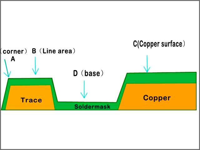
- Trace Routing: Route power and ground traces first, ensuring they are short and wide (at least 20 mils) to handle current without significant voltage drop. Signal traces for the keypad and display should be kept as direct as possible, avoiding sharp angles to reduce signal interference.
- Spacing: Maintain a minimum clearance of 10 mils between traces to prevent short circuits during manufacturing. For power traces near the battery input, a clearance of 15-20 mils is safer due to higher current.
- Board Size: Aim for a compact board, roughly 60mm x 40mm, to fit all components comfortably while keeping costs low.
Since we're limited to one layer, some connections may require jumper wires. For example, if two traces need to cross, one can be routed with a jumper soldered over the other trace. However, careful planning can reduce the need for jumpers. The final layout should be checked for errors, ensuring all connections match the schematic.
Step 5: Prototyping and Testing the Single-Sided PCB Calculator Project
After finalizing the layout, the next step in our single-sided PCB calculator project is to manufacture a prototype and test it. Here's how to proceed:
- Manufacturing: Generate the Gerber files for your PCB design and send them to a trusted fabrication service. Since it's a single-sided board, the turnaround time and cost will be minimal.
- Assembly: Solder the components onto the board, starting with the microcontroller, then the keypad, display, resistors, and capacitors. Double-check polarity for components like the display and battery holder.
- Programming: Program the microcontroller with firmware to read keypad inputs, perform calculations, and update the display. Test with simple inputs like "2 + 3 =" to ensure the output shows "5".
- Testing: Power up the board and test all functions. Check for issues like incorrect display outputs, unresponsive keys, or power supply noise. If traces are too close, you might notice crosstalk or short circuits—adjust spacing if needed.
During testing, measure the current draw to ensure it aligns with expectations. For instance, a 7-segment display with four digits might draw up to 80 mA at 5V when all segments are lit. If the current exceeds the microcontroller's pin rating (typically 20 mA per pin), consider adding driver transistors to offload the current.
Step 6: Optimizing and Finalizing the Design
Based on testing results, optimize the design for better performance or manufacturability. Here are some common optimizations:
- Reduce Power Consumption: If the calculator draws too much current, adjust the display multiplexing rate or use a lower-power microcontroller. A typical goal is to keep idle current below 1 mA for battery-powered devices.
- Improve Trace Routing: If signal noise affects keypad inputs, reroute traces to avoid running parallel to power lines, reducing electromagnetic interference.
- Enhance Durability: Add silkscreen labels for components and connectors to make assembly easier for future builds. Consider a solder mask to protect traces from oxidation.
Once optimized, the design can be finalized for small-scale production or personal use. This completed single-sided PCB calculator project serves as a practical example of how to approach simple electronics design with limited resources.
Challenges in Single-Sided PCB Calculator Design
Designing a single-sided PCB isn't without challenges, especially for compact devices like a calculator. Here are some common issues and how to address them:
- Trace Congestion: With all traces on one side, routing can become crowded. Solve this by prioritizing critical connections (like power and ground) and using jumpers sparingly for less critical signals.
- Signal Integrity: Long traces can introduce delays or noise, especially for digital signals between the keypad and microcontroller. Keep traces under 50mm where possible, and avoid routing near high-current paths.
- Component Fit: Ensure the physical size of components like the keypad and display fits the board dimensions. Always double-check footprints before finalizing the layout.
By anticipating these challenges, you can save time and avoid costly redesigns during your project.
Conclusion: Building Your Own Single-Sided PCB Calculator
Designing a single-sided PCB calculator design is a rewarding project that combines creativity and technical skill. From selecting the right single-sided PCB calculator components to drafting a single-sided PCB calculator circuit diagram, each step offers valuable learning opportunities. This case study demonstrates how a simple idea can be transformed into a functional device using basic tools and a single-sided board.
Whether you're a student, hobbyist, or professional engineer, a single-sided PCB calculator project is an excellent way to hone your skills in electronics design. With the steps outlined in this guide, you can build your own calculator, troubleshoot issues, and even customize the design for additional features like memory functions or scientific calculations.
Start small, test thoroughly, and iterate on your design. The skills you gain from this project will serve as a foundation for more complex PCB designs in the future. If you're ready to take on this challenge, gather your components and tools, and bring your calculator to life!