 ALLPCB


In the fast-paced world of electronics design, managing heat in printed circuit boards (PCBs) is a critical challenge. If you're searching for proven ways to enhance PCB cooling, thermal vias offer an effective solution. This blog post dives into thermal via case studies, PCB cooling examples, and success stories that showcase effective thermal management and real-world cooling strategies. We'll explore how thermal vias have been used to solve heat dissipation issues in various applications, backed by practical insights and data.
Why Thermal Vias Matter in PCB Cooling
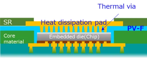
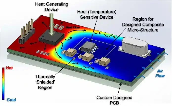
Thermal vias are small, conductive pathways in a PCB that transfer heat from one layer to another, often connecting to a ground plane or heat sink to dissipate heat efficiently. As electronic devices become smaller and more powerful, components generate more heat in confined spaces. Without proper cooling, this heat can lead to performance issues, reduced lifespan, or even complete failure of the device.
By integrating thermal vias into PCB designs, engineers can significantly improve heat dissipation. Studies have shown that well-placed thermal vias can reduce component temperatures by up to 20-30°C in high-power applications. This blog will walk you through real-world examples where thermal vias have made a measurable difference, offering actionable takeaways for your next project.
Understanding Thermal Vias: The Basics of Heat Management
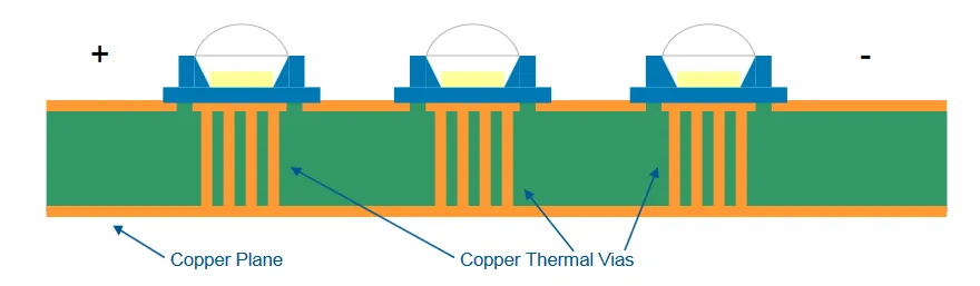
Before diving into specific case studies, let’s cover the fundamentals. Thermal vias are typically copper-plated holes that act as conduits for heat. They are strategically placed near heat-generating components, such as power transistors or microprocessors, to move heat away from critical areas. The effectiveness of thermal vias depends on factors like their diameter, spacing, and connection to thermal planes or external cooling solutions.
For instance, a common design rule is to use vias with a diameter of 0.3-0.5 mm and a spacing of 1-1.5 mm in a grid pattern under high-heat components. This setup can improve thermal conductivity by as much as 50% compared to designs without vias, according to industry benchmarks. With this foundation, let’s explore how these principles have been applied successfully in real-world scenarios.
Case Study 1: High-Power LED Lighting System
In the field of LED lighting, heat management is a top concern due to the high power density of modern LEDs. A leading manufacturer of industrial lighting systems faced a challenge: their LEDs were overheating, causing a 25% reduction in light output and a shortened lifespan of less than 10,000 hours, far below the industry standard of 50,000 hours.
The solution involved redesigning the PCB with a dense array of thermal vias beneath each LED. The vias, with a diameter of 0.4 mm and spaced 1.2 mm apart, connected the LED mounting pads to a thick copper ground plane on the bottom layer. This allowed heat to transfer efficiently away from the LEDs. Additionally, the ground plane was attached to an external aluminum heat sink for further dissipation.
The result? Post-implementation testing showed a temperature drop of 28°C at the LED junctions, restoring full light output and extending the lifespan to over 40,000 hours. This PCB cooling example highlights how thermal vias can be a game-changer in high-power applications, offering a clear lesson in effective thermal management.
Suggested Reading: Thermal Vias in LED Lighting PCBs: Keeping Your LEDs Cool and Efficient
Case Study 2: Automotive Control Module
Automotive electronics operate in harsh environments where temperature fluctuations are common. A company developing a control module for electric vehicles encountered overheating issues with their power management ICs. Under peak load, the ICs reached temperatures of 105°C, exceeding the safe operating limit of 85°C, which risked system shutdowns during operation.
The design team introduced thermal vias in a grid pattern directly under the ICs, using 0.3 mm diameter vias spaced 1 mm apart. These vias connected to an internal copper plane, which spread the heat across a larger area. To enhance cooling further, the PCB was mounted on a metal enclosure acting as a passive heat sink.
After the redesign, the IC temperatures dropped to 78°C under the same load conditions, well within safe limits. This success story demonstrates how thermal vias, combined with thoughtful board design, can tackle real-world cooling challenges in demanding environments like automotive systems.
Case Study 3: Compact Consumer Electronics Device
In the consumer electronics space, compactness often comes at the cost of heat buildup. A manufacturer of a portable streaming device faced thermal throttling issues with their processor, which reduced performance by 30% during extended use. The small form factor left little room for active cooling solutions like fans, making passive cooling essential.
The solution was to integrate thermal vias around the processor area, connecting to multiple internal copper layers for heat distribution. The vias had a diameter of 0.5 mm and were placed in a staggered pattern to maximize coverage without compromising signal integrity. This design reduced the processor temperature from 95°C to 72°C, eliminating throttling and ensuring consistent performance.
This case study is a prime example of how thermal vias can enable effective thermal management in space-constrained designs, proving their versatility across different industries. It’s a valuable thermal via case study for engineers working on compact devices.
Key Design Tips for Implementing Thermal Vias
These PCB cooling examples reveal common strategies that lead to success. Here are some practical tips to apply in your designs for optimal heat management using thermal vias:
- Placement Matters: Position thermal vias directly under or near heat-generating components to maximize heat transfer. A grid or staggered pattern often works best.
- Size and Spacing: Use vias with diameters between 0.3-0.5 mm and space them 1-1.5 mm apart. This balance ensures effective cooling without weakening the PCB structure.
- Connect to Copper Planes: Link thermal vias to large copper planes or ground layers to spread heat across a wider area. Thicker copper (e.g., 2 oz or more) enhances conductivity.
- Combine with Other Solutions: Pair thermal vias with heat sinks, metal enclosures, or thermal pads for even better results, especially in high-power designs.
- Simulation Tools: Use thermal simulation software to model heat flow and identify hotspots before fabrication. This step can save time and reduce costly redesigns.
By following these guidelines, you can replicate the success seen in the case studies above and achieve effective thermal management in your projects.
Challenges and Limitations of Thermal Vias
While thermal vias are a powerful tool, they’re not without challenges. One limitation is the potential impact on signal integrity, especially in high-frequency designs. Placing too many vias near signal traces can introduce parasitic capacitance or inductance, potentially affecting performance. For instance, in RF applications, engineers must carefully balance thermal needs with electrical constraints, often spacing vias farther from critical traces.
Another challenge is manufacturing cost. Adding numerous vias or using advanced techniques like filled vias (which improve thermal conductivity) can increase production expenses by 10-15%, depending on the complexity. However, the trade-off is often worth it when reliability and performance are on the line, as shown in the success stories we’ve discussed.
Future Trends in PCB Thermal Management
As electronics continue to evolve, so do cooling strategies. Emerging trends include the use of advanced materials like graphene for enhanced thermal conductivity, potentially outperforming copper by a factor of 10. Additionally, 3D PCB designs are gaining traction, allowing for more creative placement of thermal vias across multiple dimensions.
Another exciting development is the integration of active cooling directly into PCBs, such as embedded microchannels for liquid cooling. While still in early stages, this technology could complement thermal vias in ultra-high-power applications. Staying ahead of these trends ensures that your designs remain competitive and efficient in the long term.
Suggested Reading: The Future of Thermal Vias: Emerging Technologies in PCB Cooling
Conclusion: Leveraging Thermal Vias for Better PCB Performance
Thermal vias have proven their worth as a cornerstone of effective thermal management in PCB design. Through the thermal via case studies and PCB cooling examples shared in this post, it’s clear that they offer practical, measurable benefits across industries—from LED lighting to automotive and consumer electronics. These success stories underscore the importance of strategic design in solving real-world cooling challenges.
Whether you’re dealing with high-power components or compact devices, incorporating thermal vias can significantly enhance performance and reliability. By applying the design tips and lessons from these case studies, you can create PCBs that stand up to the heat—literally. Trust in proven strategies and innovative thinking to keep your designs cool and efficient for years to come.


